1.2.2 The Memory Subsystem
A typical 80x86 processor addresses a maximum of 2n different memory locations, where n is the number of bits on the address bus1. As you've seen already, 80x86 processors have 20, 24, 32, and 36 bit address busses (with 64 bits on the way).
Of course, the first question you should ask is, "What exactly is a memory location?" The 80x86 supports byte addressable memory. Therefore, the basic memory unit is a byte. So with 20, 24, 32, and 36 address lines, the 80x86 processors can address one megabyte, 16 megabytes, four gigabytes, and 64 gigabytes of memory, respectively.
Think of memory as a linear array of bytes. The address of the first byte is zero and the address of the last byte is 2n-1. For an 8088 with a 20 bit address bus, the following pseudo-Pascal array declaration is a good approximation of memory:
Memory: array [0..1048575] of byte;
To execute the equivalent of the Pascal statement "Memory [125] := 0;" the CPU places the value zero on the data bus, the address 125 on the address bus, and asserts the write line (since the CPU is writing data to memory), see Figure 1.2.
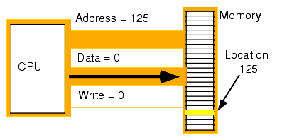
Figure 1.2 Memory Write Operation
To execute the equivalent of "CPU := Memory [125];" the CPU places the address 125 on the address bus, asserts the read line (since the CPU is reading data from memory), and then reads the resulting data from the data bus (see Figure 1.3).
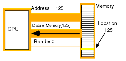
Figure 1.3 Memory Read Operation
The above discussion applies only when accessing a single byte in memory. So what happens when the processor accesses a word or a double word? Since memory consists of an array of bytes, how can we possibly deal with values larger than eight bits?
Different computer systems have different solutions to this problem. The 80x86 family deals with this problem by storing the L.O. byte of a word at the address specified and the H.O. byte at the next location. Therefore, a word consumes two consecutive memory addresses (as you would expect, since a word consists of two bytes). Similarly, a double word consumes four consecutive memory locations. The address for the double word is the address of its L.O. byte. The remaining three bytes follow this L.O. byte, with the H.O. byte appearing at the address of the double word plus three (see Figure 1.4). Bytes, words, and double words may begin at any valid address in memory. We will soon see, however, that starting larger objects at an arbitrary address is not a good idea.
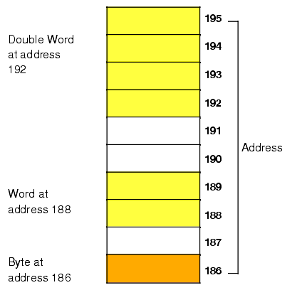
Figure 1.4 Byte, Word, and DWord Storage in Memory
Note that it is quite possible for byte, word, and double word values to overlap in memory. For example, in Figure 1.4 you could have a word variable beginning at address 193, a byte variable at address 194, and a double word value beginning at address 192. These variables would all overlap.
A processor with an eight-bit bus (like the old 8088 CPU) can transfer eight bits of data at a time. Since each memory address corresponds to an eight bit byte, this turns out to be the most convenient arrangement (from the hardware perspective), see Figure 1.5.
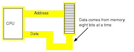
Figure 1.5 Eight-Bit CPU <-> Memory Interface
The term "byte addressable memory array" means that the CPU can address memory in chunks as small as a single byte. It also means that this is the smallest unit of memory you can access at once with the processor. That is, if the processor wants to access a four bit value, it must read eight bits and then ignore the extra four bits. Also realize that byte addressability does not imply that the CPU can access eight bits on any arbitrary bit boundary. When you specify address 125 in memory, you get the entire eight bits at that address, nothing less, nothing more. Addresses are integers; you cannot, for example, specify address 125.5 to fetch fewer than eight bits.
CPUs with an eight-bit bus can manipulate word and double word values, even through their data bus is only eight bits wide. However, this requires multiple memory operations because these processors can only move eight bits of data at once. To load a word requires two memory operations; to load a double word requires four memory operations.
Some older x86 CPUs (e.g., the 8086 and 80286) have a 16 bit data bus. This allows these processors to access twice as much memory in the same amount of time as their eight bit brethren. These processors organize memory into two banks: an "even" bank and an "odd" bank (see Figure 1.6). Figure 1.7 illustrates the connection to the CPU (D0-D7 denotes the L.O. byte of the data bus, D8-D15 denotes the H.O. byte of the data bus):
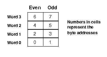
Figure 1.6 Byte Addressing in Word Memory
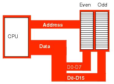
Figure 1.7 Sixteen-Bit Processor (8086, 80186, 80286, 80386sx) Memory Organization
The 16 bit members of the 80x86 family can load a word from any arbitrary address. As mentioned earlier, the processor fetches the L.O. byte of the value from the address specified and the H.O. byte from the next consecutive address. This creates a subtle problem if you look closely at the diagram above. What happens when you access a word on an odd address? Suppose you want to read a word from location 125. Okay, the L.O. byte of the word comes from location 125 and the H.O. word comes from location 126. What's the big deal? It turns out that there are two problems with this approach.
First, look again at Figure 1.7. Data bus lines eight through 15 (the H.O. byte) connect to the odd bank, and data bus lines zero through seven (the L.O. byte) connect to the even bank. Accessing memory location 125 will transfer data to the CPU on the H.O. byte of the data bus; yet we want this data in the L.O. byte! Fortunately, the 80x86 CPUs recognize this situation and automatically transfer the data on D8-D15 to the L.O. byte.
The second problem is even more obscure. When accessing words, we're really accessing two separate bytes, each of which has its own byte address. So the question arises, "What address appears on the address bus?" The 16 bit 80x86 CPUs always place even addresses on the bus. Even bytes always appear on data lines D0-D7 and the odd bytes always appear on data lines D8-D15. If you access a word at an even address, the CPU can bring in the entire 16 bit chunk in one memory operation. Likewise, if you access a single byte, the CPU activates the appropriate bank (using a "byte enable" control line). If the byte appeared at an odd address, the CPU will automatically move it from the H.O. byte on the bus to the L.O. byte.
So what happens when the CPU accesses a word at an odd address, like the example given earlier? Well, the CPU cannot place the address 125 onto the address bus and read the 16 bits from memory. There are no odd addresses coming out of a 16 bit 80x86 CPU. The addresses are always even. So if you try to put 125 on the address bus, this will put 124 on to the address bus. Were you to read the 16 bits at this address, you would get the word at addresses 124 (L.O. byte) and 125 (H.O. byte) - not what you'd expect. Accessing a word at an odd address requires two memory operations. First the CPU must read the byte at address 125, then it needs to read the byte at address 126. Finally, it needs to swap the positions of these bytes internally since both entered the CPU on the wrong half of the data bus.
Fortunately, the 16 bit 80x86 CPUs hide these details from you. Your programs can access words at any address and the CPU will properly access and swap (if necessary) the data in memory. However, to access a word at an odd address requires two memory operations (just like the 8088/80188). Therefore, accessing words at odd addresses on a 16 bit processor is slower than accessing words at even addresses. By carefully arranging how you use memory, you can improve the speed of your program on these CPUs.
Accessing 32 bit quantities always takes at least two memory operations on the 16 bit processors. If you access a 32 bit quantity at an odd address, a 16-bit processor will require three memory operations to access the data.
The 80x86 processors with a 32-bit data bus (e.g., the 80386 and 80486) use four banks of memory connected to the 32 bit data bus (see Figure 1.8).
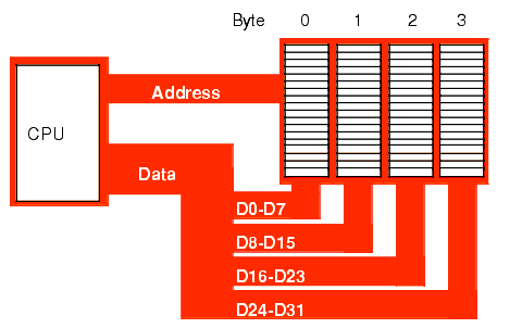
Figure 1.8 32-Bit Processor (80386, 80486, Pentium Overdrive) Memory Organization
The address placed on the address bus is always some multiple of four. Using various "byte enable" lines, the CPU can select which of the four bytes at that address the software wants to access. As with the 16 bit processor, the CPU will automatically rearrange bytes as necessary.
With a 32 bit memory interface, the 80x86 CPU can access any byte with one memory operation. If (address MOD 4) does not equal three, then a 32 bit CPU can access a word at that address using a single memory operation. However, if the remainder is three, then it will take two memory operations to access that word (see Figure 1.9). This is the same problem encountered with the 16 bit processor, except it occurs half as often.
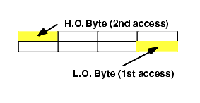
Figure 1.9 Accessing a Word at (Address mod 4) = 3.
A 32 bit CPU can access a double word in a single memory operation if the address of that value is evenly divisible by four. If not, the CPU will require two memory operations.
Once again, the CPU handles all of this automatically. In terms of loading correct data the CPU handles everything for you. However, there is a performance benefit to proper data alignment. As a general rule you should always place word values at even addresses and double word values at addresses which are evenly divisible by four. This will speed up your program.
The Pentium and later processors provide a 64-bit bit data bus and special cache memory that reduces the impact of non-aligned data access. Although there may still be a penalty for accessing data at an inappropriate address, modern x86 CPUs suffer from the problem less frequently than the earlier CPUs. The discussion of cache memory in a later chapter will discuss the details.
1.2.3 The I/O Subsystem
Besides the 20, 24, or 32 address lines which access memory, the 80x86 family provides a 16 bit I/O address bus. This gives the 80x86 CPUs two separate address spaces: one for memory and one for I/O operations. Lines on the control bus differentiate between memory and I/O addresses. Other than separate control lines and a smaller bus, I/O addressing behaves exactly like memory addressing. Memory and I/O devices both share the same data bus and the L.O. 16 lines on the address bus.
There are three limitations to the I/O subsystem on the PC: first, the 80x86 CPUs require special instructions to access I/O devices; second, the designers of the PC used the "best" I/O locations for their own purposes, forcing third party developers to use less accessible locations; third, 80x86 systems can address no more than 65,536 (216) I/O addresses. When you consider that a typical video display card requires over eight megabytes of addressable locations, you can see a problem with the size of I/O bus.
Fortunately, hardware designers can map their I/O devices into the memory address space as easily as they can the I/O address space. So by using the appropriate circuitry, they can make their I/O devices look just like memory. This is how, for example, display adapters on the PC work.
1This is the maximum. Most computer systems built around 80x86 family do not include the maximum addressable amount of memory.
|