
Note: All photographs appearing on this page are freely usable for any purpose. Links to high-resolution versions of the pictures appear below each picture.
Digital Data Acquisition & Control System
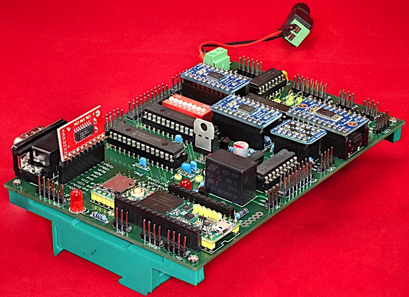
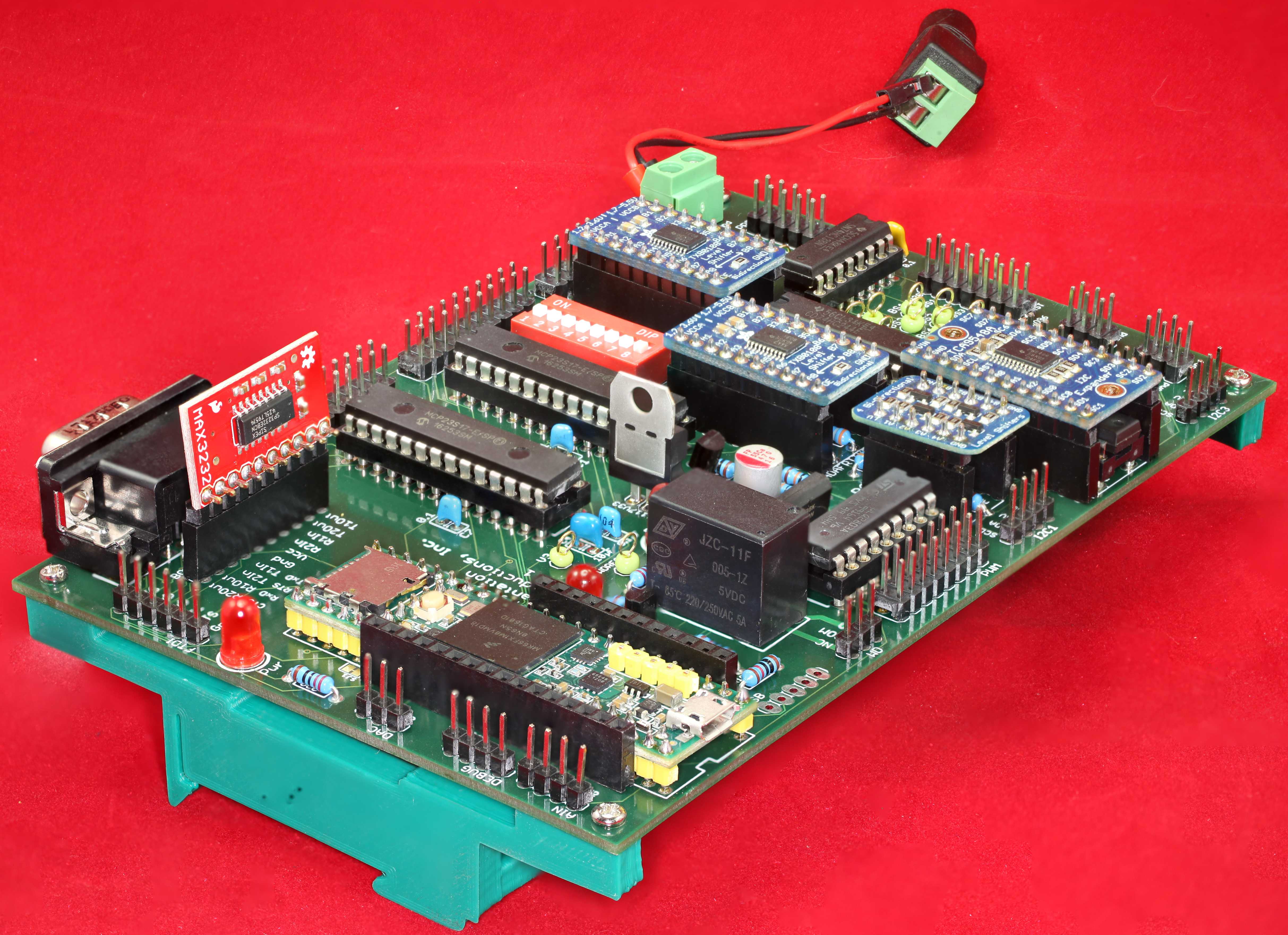
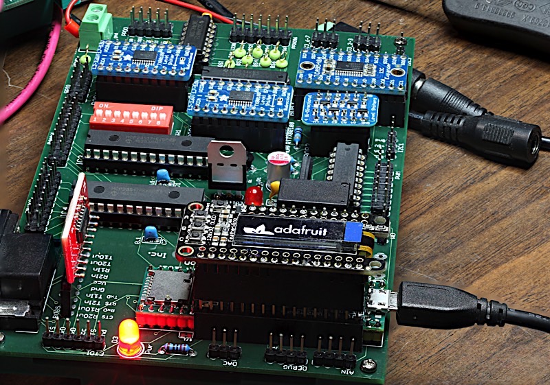
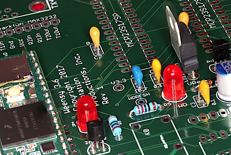
Weensy 3.6
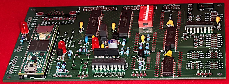
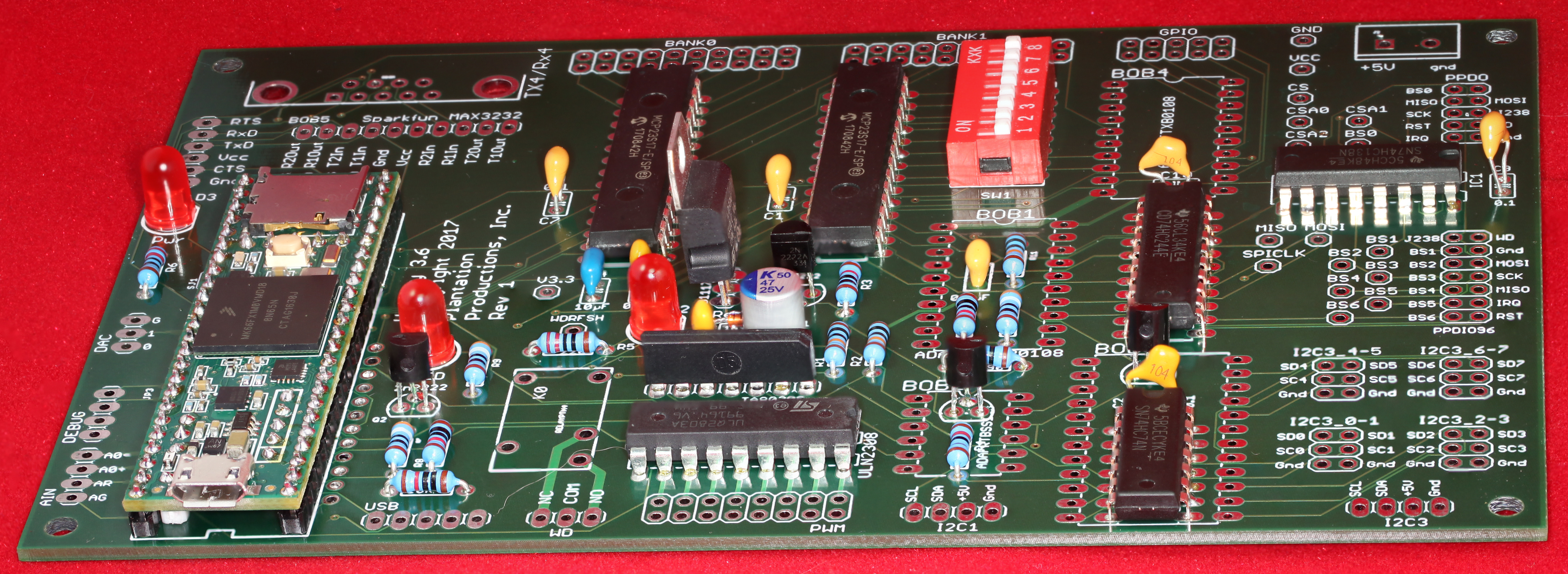
Breakout board and I/O Expansion for Teensy 3.6
High-resolution image shot with a Canon EOS 5D MII
The latest revision of the Weensy 3.6 circuit board (Rev 4) has been submitted to the PCB house on Sept 8, 2017. It takes about 4-6 weeks to get the boards back. Until further notice, be aware that the Rev 4 files provided here are untested. Until the boards arrive and I can test them, I do not recomend making a production run of these boards. Please treat this information as a "call for comments" until I can fully test the Rev 4 boards.
Randy Hyde (randy hyde at earth link dot net) -- Remove spaces and make appropriate changes (a feeble attempt to get around the spam bots; no doubt AI has progressed to the point they figure this out anyway, but I try...)
Note: The Weensy 3.6 hardware and software are covered under the Creative Commons Attribution 4.0 International license.
Here is the "normal person"-readable version of that license.
Here is the version for lawyers.
For more information on Creative Commons, visit their website.
For the purposes of attribution,
Copyright 2017
Plantation Productions, Inc.
Randall Hyde
Note: disclaimer of warranty appears in the legal version of the license.
Table of Contents
Overview
The Weensy 3.6 board is a breakout board and I/O expansion for the Teensy 3.6 from PJRC. It provides the following features:
- Open Hardware design based on Creative Commons 4.0 license
- Single 5V power supply input connector (screw terminals); provides 3.3V for Teensy 3.6 and other peripherals.
- LED indicates when power is applied.
- Adafruit-compatible Feather bus (compatible with software written for the feather adapter for the Teensy 3.2).
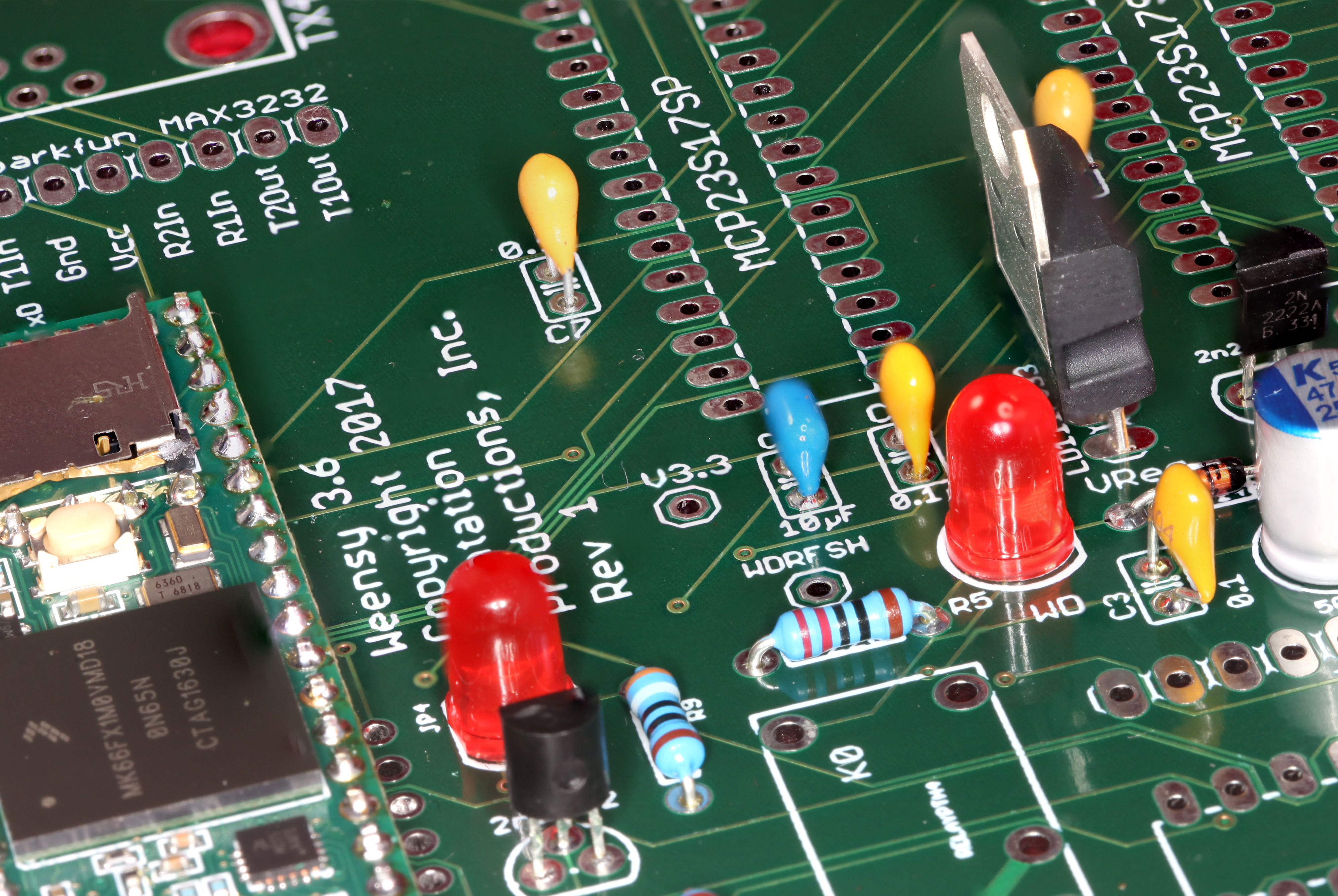
- Two MCP23S17 GPIO expansion chips provide 24 I/O lines (presented on two PPDIO96-compatible 20-pin headers) and eight DIP switches.
- PPDIO96 compatible connectors support PPOPTO-12 opto-isolator and PPRLYIO-12 relay-based input boards.
- Eight PWM-compatible digital output lines are routed through a ULN2308 darlington array (high-current, 500ma/pin).
- Eight Teensy 3.6 GPIO pins are brought out to a header through a 5V level shifter.
- Watchdog timer actuates a relay after five-second timeout without a refresh operation (timeout period can be changed by swapping out a different resistor).
- An LED indicates current watchdog timeout state.
- Watchdog state (relay) is available on a three-pin header (relay NO, COM, and NC contact signals).
- An LED indicates when the watchdog timer is being refreshed.
- 3.3V level shifting (from Teensy 3.6) to 5V for many I/O pins.
- RS232 level shifting (from TTL to RS-232 levels) for one RS-232 serial port (using Sparkfun Max3232 or FTDI cable).
- I2C level shifting for two I2C ports (one of which is multiplexed to eight ports).
- Provides 8 independent I2C ports (routed to four six-pin headers on the board).
- I2C expansion bus connectors support PPAIO-16/4 analog I/O boards (as well as PPAC-4 and PPAC420 analog conditioning boards).
- SPI bus expansion with eight independent chip select lines (routed to two headers on the board -- PPDIO96 bus and PPDO bus; note: one CS line controls the two on-board MCP23S17 GPIO expanders).
- PPDIO96-compatible bus supports up to six PPDIO96 digital I/O boards (96 digital I/O lines/board, up to 576 additional I/O lines!).
- PPDO-compatible bus supports up to 10 PPRelay-12 and/or PPSSR-16 relay/digital output boards.
- Headers for Teensy 3.6 analog input (ADC) ports.
- Headers for Teensy 3.6 analog output (DAC) ports.
- Headers for Teensy 3.6 USB Host port.
- Full buffering for output signals.
- Interrupt support for digital input devices.
- Test pins for various important signals are present on the PCB.
- Software-controlled reset line for resetting peripherals.
- Watchdog state is also broadcast to all peripheral boards.
- Schematic and board layout are available in Eagle format.
- DIN rail brackets are available in .STL format for 3D-printing.
Bill of Materials
Bill of Materials (BOM) for the Weensy 3.6board:
- (1) Teensy 3.6 CPU module
- (1) 5x2 SMT male header
- (1) 4x2 SMT male header
- (1) 3x2 SMT male header
- (2) 10x2 pin male header
- (1) 8x2 pin male header
- (1) 7x2 pin male header
- (2) 5x2 pin male header
- (4) 3x2 pin male header
- (2) 24x1 pin male header
- (1) 16x1 pin male header
- (1) 12x1 pin male header
- (1) 10x1 pin male header
- (1) 6x1 pin male header
- (2) 5x1 pin male header
- (4) 4x1 pin male header
- (3) 3x1 pin male header
- (1) DB9M PCB-mount 9-pin serial connector
- (1) 2-pin 5mm center screw terminal
- (1) LD1117V33 voltage regulator (3.3v)
- (4) 2N2222 NPN transistor
- (3) 5mm red LED
- (4) 100 kΩ resistor
- (4) 10 kΩ resistor
- (1) 1 kΩ resistor
- (4) 390 Ω resistor
- (2) 220 Ω resistor
- (1) 27 Ω resistor
- (1) 47 µF capacitor
- (1) 10 µF capacitor
- (8) 0.1 µF capacitor
- (1) 1N4148 diode
- (1) 1N4728A zener diode (4.5 to 5V)
- (1) ULN2308 Darlington transistor array
- (1) Toshiba TA8030S watchdog timer
- (1) JZC-11F-05VDC-1Z relay (Sparkfun)
- (2) MCP23S17 SPI GPIO Expander
- (1) 74HC74 flip-flop
- (1) 74HC138 demultiplexer/1-of-8 decoder
- (1) 74HC244 Octal Buffer
- (1) 8-position DIP switch
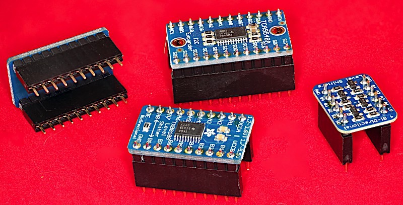
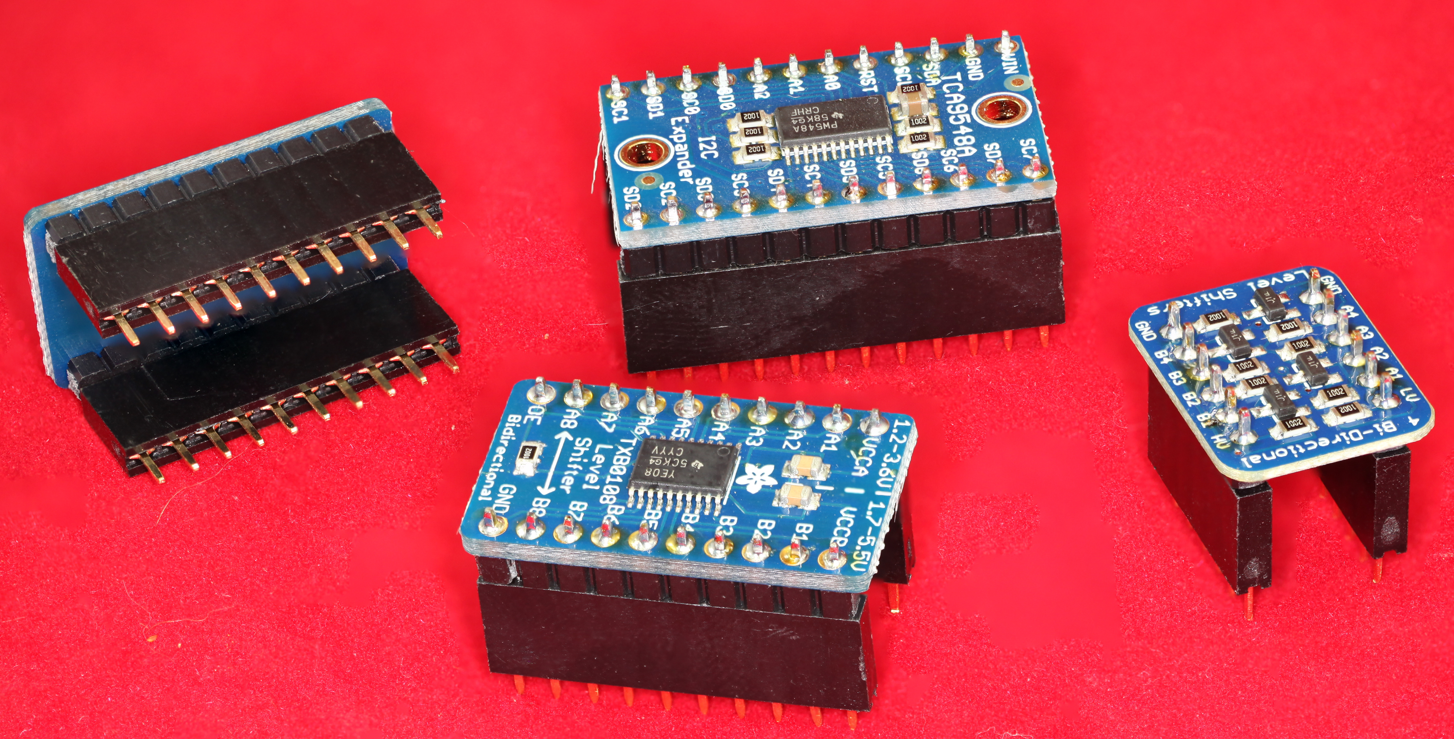
- (2) Adafruit TXB0108 bi-directional level shifter
- (1) Adafruit BSS138 bi-directional level shifter
- (1) Adafruit TCA9548A I2C multiplexer
- Optional: (1) Sparkfun MAX3232 RS-232 level shifter
- Optional: (20) test pins
- Optional: one set of horizontal 35mm DIN rail mounts for DAQ boards
Note: If you only want a few Weensy 3.6 PCBs, contact Plantation Productions (randy@plantation-productions.com) to see if there are any in stock. Bare boards are $25 each plus shipping; fully assembled and tested boards are $699. If you need more than a couple PCBs and you're not in a huge hurry, it costs about $150 (plus about 4-6 weeks) to have a set of 10 manufactured and shipped to you from China. I use Seeed Studio Fusion PCD service (https://www.seeedstudio.com/fusion.html).
Weensy 3.6 Files
The Weensy 3.6 PCBs are four-layer boards. Here are the Gerber files for them (provide these files to Seeed Studio or your personal PCB manufacturer).
If you want to modify or enhance the DAQ_IF design, or re-layout the PCB using Eagle, here are the Eagle files:
Weensy 3.6 Eagle files (Schematic and board layout)
If you simply want to view the schematic on-line, you'll find that here:
The DIN rails were created using AutoDesk's Fusion 360 (to produce STL files) and I personally print the results on a Lulzbot Taz6 3D printer using ABS filament (ABS is recommended for this job, PLA and PETG are a bit brittle). The STL files can be found here:
Weensy 3.6 DIN Rail Brackets 3D printer files
Weensy 3.6 Board Layout
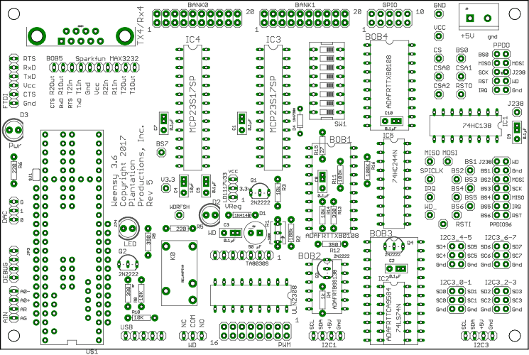
Weensy 3.6 Eagle Files
The Weensy 3.6 Eagle PCB files contain two sets of files: weensy.sch/weensy.brd and weensy.MT.sch/weensy.MT.brd. The *.MT.* files (MT="Manual Traces") contain some manually inserted traces that handle important signals requiring special layouts (specifically, the high-current traces from the watchdog relay to the three-pin connector). If you want to make changes to the board layout, make them to the *.MT.* files; then copy the weensy.MT.sch and weensy.MT.brd files to the weensy.sch and weensy.brd files (respectively) and run the auto-router on them. When running the autorouter, be sure to load the Weensy.ctl file that applies higher costs to the inner layers (which should be power and ground only) and a few other routing rules.
Weensy 3.6 Revisions History
Rev 1:
Reversed pins on small Feather connector.
Added resistor and cap to WD reset line to prevent
constant reset when held low.
Added 74HC244 buffer for various SPI and other output lines.
Rev 2:
Modified reset circuit on 7474 --
Moved resistor to 3.3V and added a clamping diode/resistor
to prevent overvoltage.
Rev 3:
Added 3-pad decoupling capactors to allow 0.2" and 0.3" center caps.
Put wider traces on the relay.
Ran INTA pins on mcp23S17 ICs through the level shifter.
Rev 4:
Added pin number silk screen to Bank pins. Added additional test points
Changed MCP23S17 SPI control lines to 5V logic. Added Pot overlay
for R1 (WD time constant).
Rev 5:
Changed BS7 label to RSTO (bad label).
Added RSTI test pin.
Changed Reset lines on MCP23s17 ICs to DI_RESET and DO_RESET.
Changed R2 from 100K to 10K.
Rev 6:
Inverted output from WD timer to produce failsafe WD output
(must use NO contacts rather than NC contacts, now). Now when
power is not applied, relay is open; when WD times out, relay is open.
Changed label on Watchdog LED from "WD" to "WD Safe".
Weensy 3.6 Functionality
The Weensy 3.6 board provides the following functionality:
- Almost all pins on the Teensy 3.6 are brought out to various connectors or circuits on the Weensy 3.6 board.
- Adafruit Feather compatible bus - Electrically identical to the Teensy 3.2 Feather adapter from Adafruit.
- Level shifting: The Weensy 3.6 board converts 3.3V logic levels to the 5V logic levels for all external connections (except Feather interface bus which is 3.3V).
- I2C level shifting: The Weensy 3.6 board converts I2C signals on two of the three I2C busses brought out from 3.3V and 5V (note: the I2C bus on the Feather interface bus operates at 3.3V as per the Feather specs).
- Two SPI busses available: one on the Feather interface bus and one providing a DAQ_IF-compatible PPDIO96 and PPDO SPI expansion bus.
- SPI bus expansion: The Weensy 3.6 board expands the SPI chip-select line to eight separate board select lines (BS0, BS1,..., BS7).
- I2C bus expansion: The Weensy 3.6 board contains an Adafruit TCA9584 I2C bus multiplexor breakout board that expands one of the I2C busses to eight separate I2C busses (allowing you to attach up to eight devices with the same I2C bus to the Weensy 3.6 board).
- RS-232 level shifting: The Weensy 3.6 board includes a Sparkfun Max3232 breakout board that converts TTL-level RS-232 signals to true RS-232.A DB-9 DTE connection is provided on the Weensy 3.6 board.
- FTDI support: In place of the MAX3232 module, you can optionally install an FTDI serial-to-USB cable. Note: only one of the MAX3232 module or FTDI cable may be installed on a single Weensy 3.6 board. Installing both of these devices will create conflicts that could damage the modules or the Weensy 3.6 board.
- Five second watchdog timer with SPDT NC/COM/NO (normally closed/common/normally open) relay. Useful in safety critical systems to detect when the software has frozen. Hardware can automatically reset itself or place the system in a fail-safe mode when a watchdog timeout occurs. Timeout is nominally 5 seconds but you can easily change it by substituting a different resistor value.
- Buffering for all output signals (including SPI outputs).
In addition to the above, the Weensy 3.6 board features LEDs indicating the following:
- Power applied
- Watchdog timeout
- Heartbeat/watchdog refresh/general purpose LED output
The Weensy 3.6 board also includes numerous test pins to aid in testing and maintenance of the board.
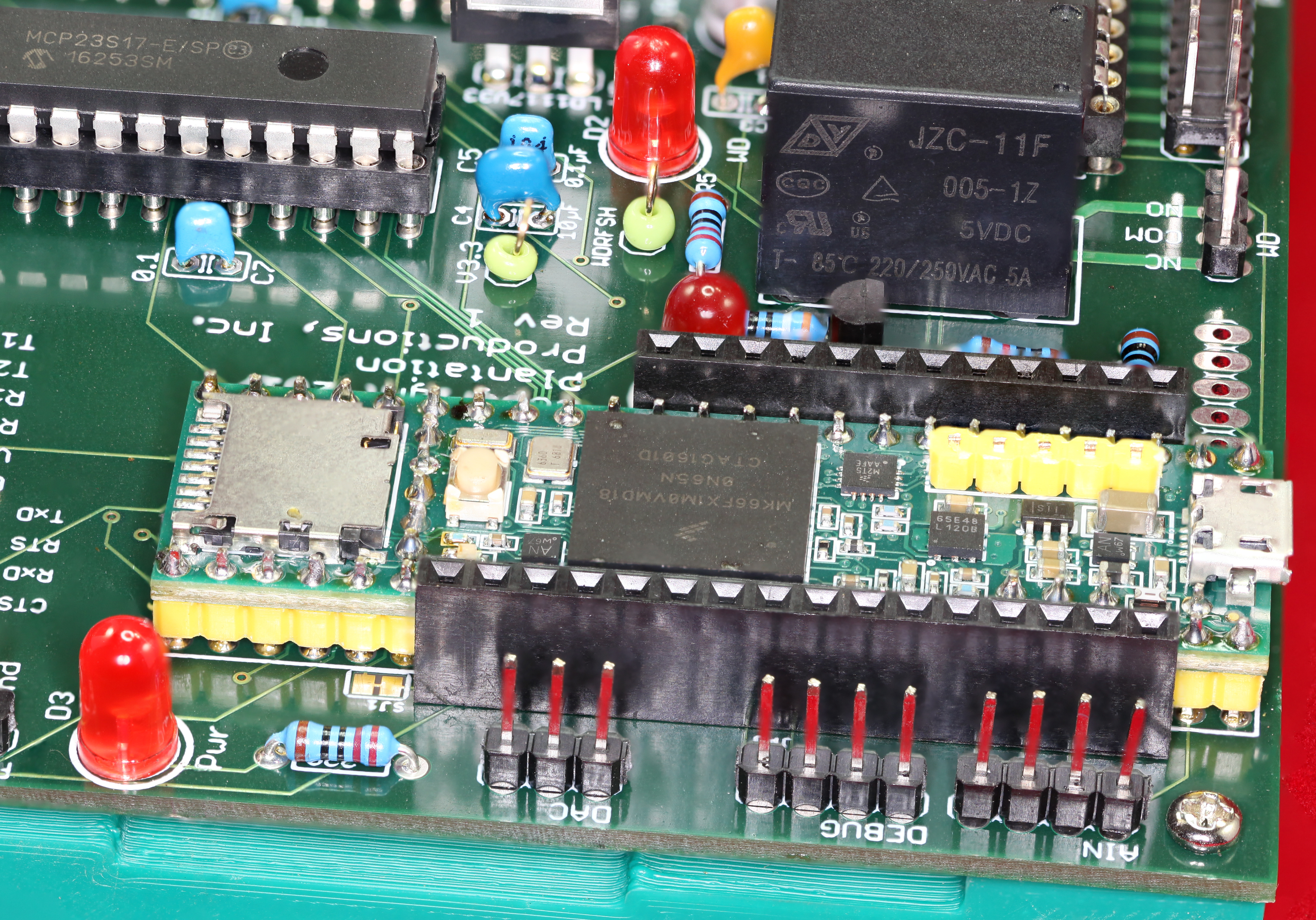
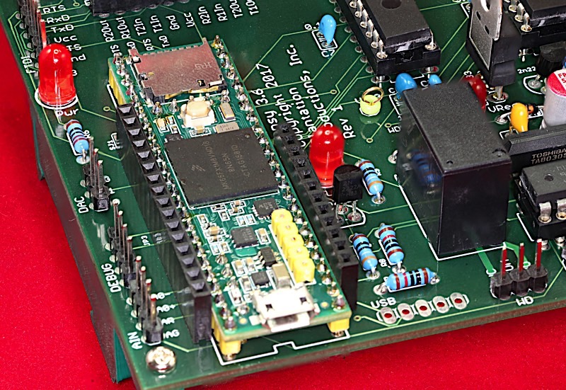
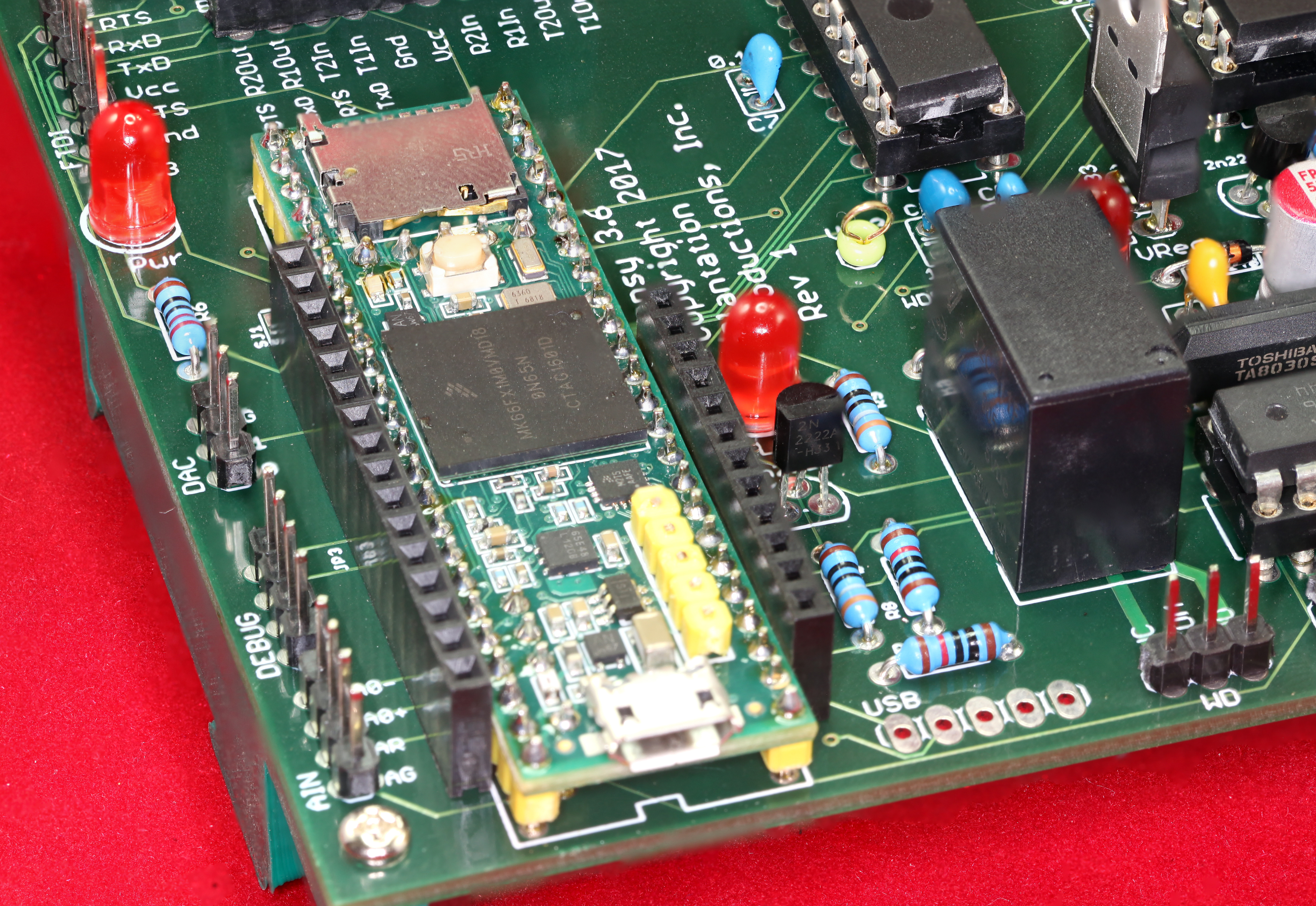
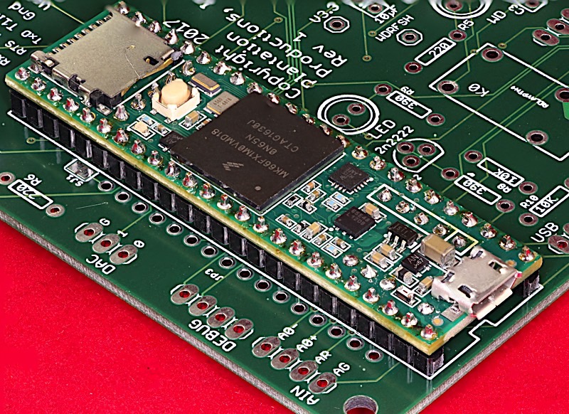
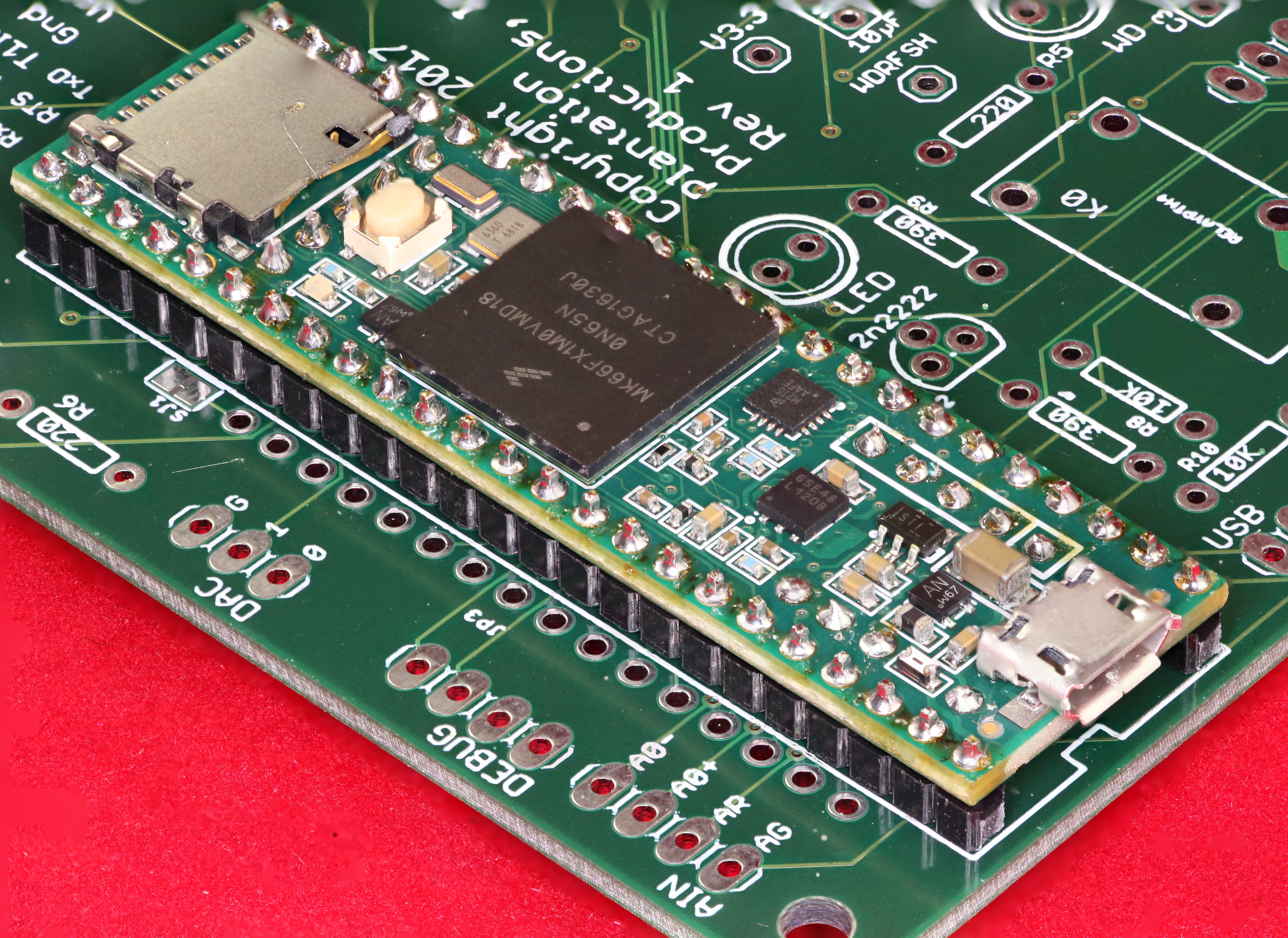
Components on the Weensy 3.6 Board
Teensy 3.6 and Feather bus
High-resolution image shot with a Canon EOS 5D MII
High-resolution image shot with a Canon EOS 5D MII
The Weensy 3.6 brings out a set of two headers that are physically and electrically compatible with the Adafruit Feather bus as implemented on Adafruit's Teensy 3.2 Feather adapter.
The Adafruit Feather bus headers (JP3 and JP4) straddle the Teensy 3.6 CPU board on the Weensy 3.6:
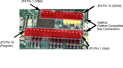
The Feather bus is a 3.3V I/O bus support digital and analog I/O as well as SPI and I2C periperals (also 3.3V). The pinouts for the Feather bus are as follows:
| Pin | Function |
|---|---|
| 1 | Gnd |
| 2 | TX1 |
| 3 | RX1 |
| 4 | MISO0 |
| 5 | MOSI0 |
| 6 | SCK0 |
| 7 | A6 (analog input 0-3.3V) |
| 8 | A0 (analog input 0-3.3V) |
| 9 | A2 (analog input 0-3.3V) |
| 10 | A3 (analog input 0-3.3V) |
| 11 | A1 (analog input 0-3.3V) |
| 12 | DAC0 |
| 13 | Gnd |
| 14 | ARef |
| 15 | 3.3v supply (max 250mA) |
| 16 | Program |
| Pin | Function |
|---|---|
| 1 | VBat |
| 2 | N/C |
| 3 | Vcc (3.3v) |
| 4 | Digital I/O pin 5 (3.3v only) |
| 5 | Digital I/O pin 6 (3.3v only) |
| 6 | Digital I/O pin 9 (3.3v only) |
| 7 | Digital I/O pin 10 (3.3v only) |
| 8 | Digital I/O pin 4 (3.3v only) |
| 9 | Digital I/O pin 3 (3.3v only) |
| 10 | Digital I/O pin 8 (3.3v only) |
| 11 | SCL0 (3.3v, with 10K pullup to +3.3v) |
| 12 | SDA0 (3.3v, with 10K pullup to +3.3v) |
Note that the Teensy 3.6 has two actual A/D converters that it multiplexes amongst all the "A*" pins on the Teensy 3.6. In particular the Teensy multiplexes the A0, A1, A2, A3, and A6 on the Feather bus to these two A/D converters. The Weensy 3.6 brings out pins A10 and A11 to a four-pin header next to the Teensy 3.6 (and Feather connectors). Because the Weensy 3.6 can interface with Plantation Productions' PPAIO16/4 board (16 analog inputs and four analog outputs) the Weensy doesn't really need for a large number of (multiplexed) analog inputs. The design intent is to use A10 and A11 on the analog input headers when using the Teensy 3.6 on-board ADCs (with no multiplexing taking place). The A0-A3 and A6 pins are supported on the Feather bus to maintain compatibility with the bus.
Adafruit sells a variety of "Feather Wings", which are little I/O modules, that plug into a Feather bus connector. Most of these are compatible with the Feather bus implementation on the Weensy 3.6. Examples of useful Featherwings include:
- Adafruit Feather Huzzah w/ESP7266 WiFi
- Adafruit Featherwing proto boards
- Adalogger Featherwing
- Featherwing OLED
- Adafruit Ultimate GPS Featherwing
- Adafruit Power Relay Featherwing
- Adafruit DS3231 Precision RTC Featherwing
- Adafruit TFT Featherwing (2.4" touchscreen)
- Adafruit DC Motor+Stepper Featherwing
- Adafruit Featherwing doubler
- Adafruit Neopixel Featherwing
- Adafruit Non-latching Mini Relay Featherwing
- Adafruit LoRa Radio Featherwing
- Adafruit Ethernet Featherwing
- Adafruit Terminal Block Featherwing
- Adafruit 8-channel PWM/Servo Featherwing
- Adafruit 8x16 LED Matrix Featherwing
- Adafruit 7-segment display Featherwing
- Adafruit Musicmaker Featherwing
- Adafruit CharliePlex 15x7 LED matrix display Featherwing
- Adafruit Quad Alphanumeric Featherwing
- More stuff appearing all the time
For more information, visit the Adafruit Feather web page: https://www.adafruit.com/category/943.
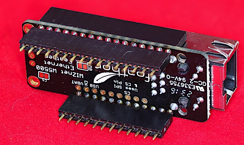
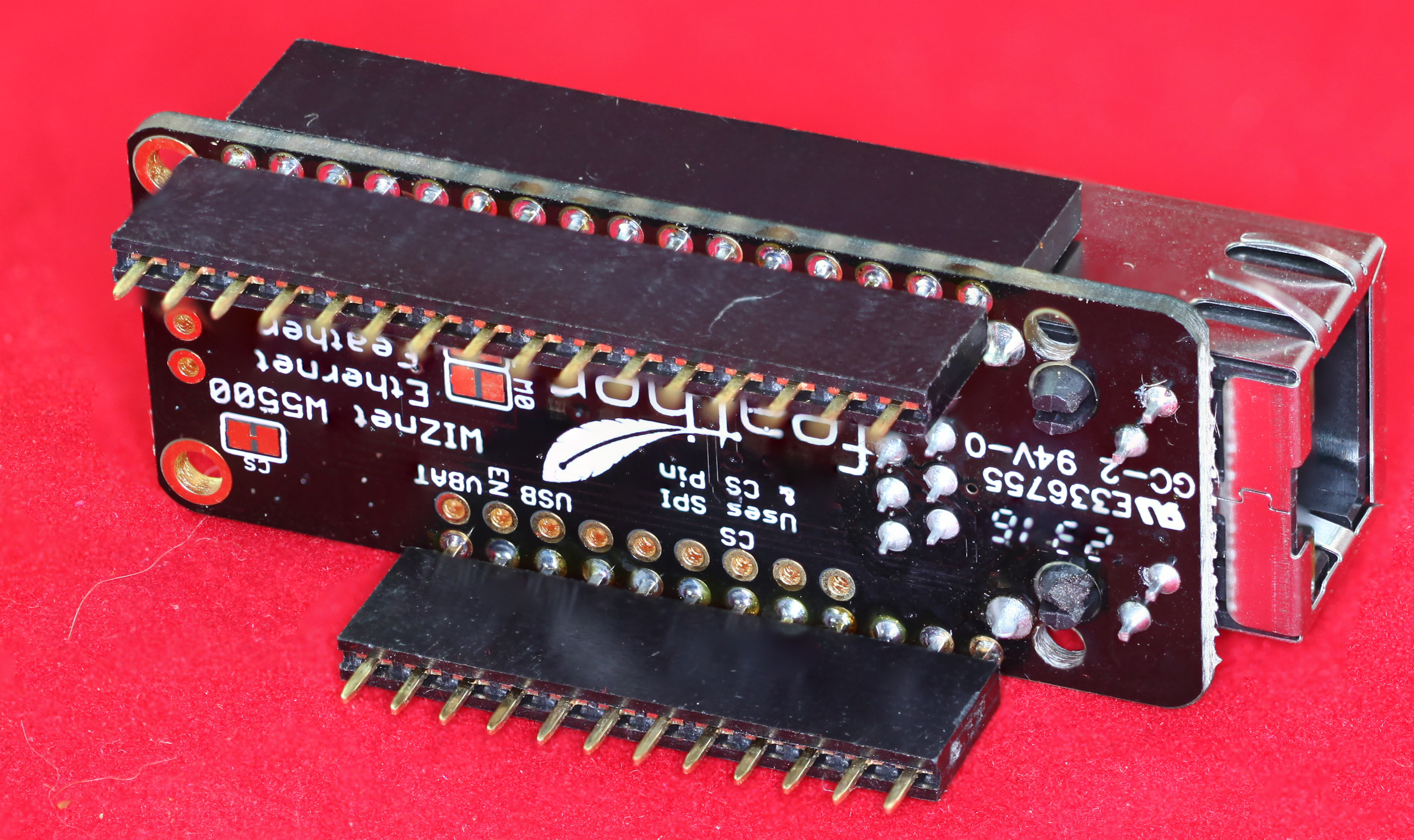
The Ethernet Featherwing and OLED Featherwing are especially useful on the Weensy 3.6 board. Here's the Adafruit OLED Featherwing running on a Weensy 3.6 (this is running the Adafruit OLED test program):
High-resolution image shot with a Canon EOS 5D MII
Weensy 3.6 with Adafruit Ethernet Featherwing installed:
High-resolution image shot with a Canon EOS 5D MII
ADC and DAC Ports on the Weensy 3.6
The Teensy 3.6 supports up to 25 analog input pins (A0-A24). The chip itself does not have 25 analog-to-digital converters (ADCs); instead, the Teensy 3.6's CPU has two ADCs that you can mulitiplex across all the analog pins. Every analog input pin except pins A10 and A11 have multiple purposes. The Weensy 3.6 tends to use those pins (that support analog input) as their "alternate function". Therefore, the Weensy 3.6 associates the two actual ADC ports with A10 and A11, which do not have multiple functions associated with them.
Although the basic design philosophy of the Weensy 3.6 is to provide only two analog input pins (A10 & A11), there is an exception to this rule: A0, A1, A2, A3, and A6 are brought out on the Adafruit Feather bus. As such, these pins can be used as analog input pins (or as one of their alternate functions) as desired by a Featherwing attached to the Feather bus (and the corresponding software manipulating that peripheral).
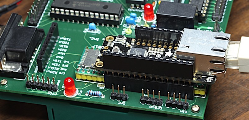
The Weensy 3.6 brings out the A10 & A11 pins (along with AGnd and ARef) to the AIN header next to the Teensy 3.6 CPU board:
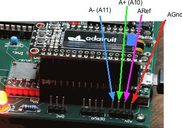
The A10 & A11 pins can provide two single-ended analog inputs or you can use the pair of them to provide a differential (double-ended) analog input. When operating in differential mode, A10 is the positive (+) input and A11 is the negative (-) input. When using single-ended inputs, the input voltage must be between 0v and 3.3v with respect to the analog ground (AGnd) pin.
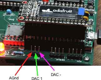
The Teensy 3.6 also provides two 12-bit digital-to-analog converters (DACs): DAC0 and DAC1. These signals, along with an analog ground, appear on the DAC header next to the Teensy 3.6 CPU board (expect to see a voltage in the range 0v to 3.3v on these pins). Note that DAC 0 is also brought out on pin 12 of JP3 on the Feather bus.
Watchdog Control on the Weensy 3.6
The Weensy 3.6 has a watchdog timer on board. Note that this watchdog timer is different from the one built into the CPU on the Teensy 3.6 board; the Teensy's watchdog timer (when appropriately programmed) will reset the CPU if the watchdog timer times out. The watchdog timer on the Weensy 3.6 board actuates a relay if the watchdog timer expires.
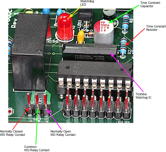
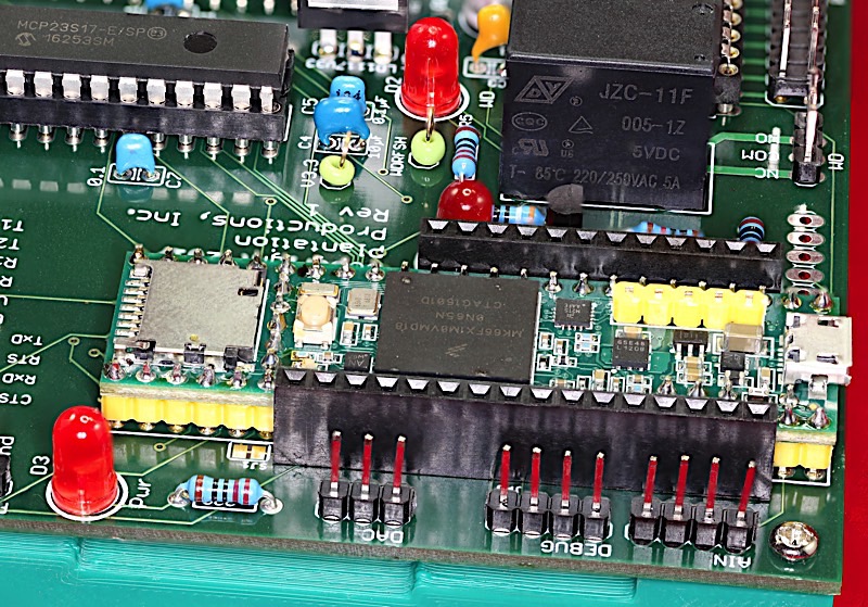
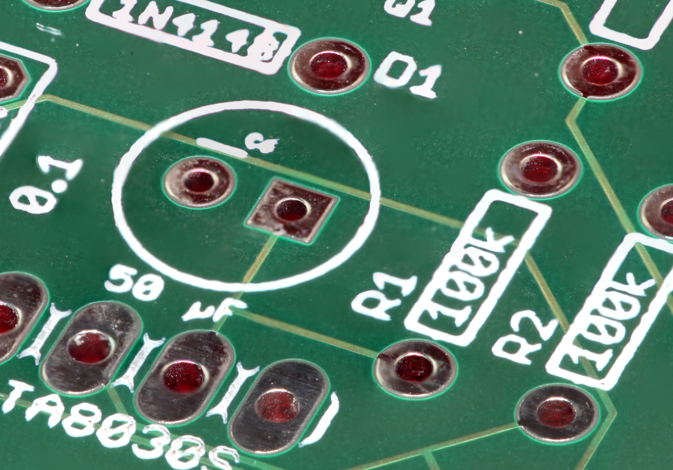
The Toshiba TAB030S watchdog timer IC determines its timeout period via an RC (resistor-capacitor) circuit. R1 on the Weensy 3.6 board (nominally 100 kΩ) and the 47 µF capacitor next two determine the timeout period (100,000 * 0.000047 is 4.7 seconds). If you want to change the timeout period, the best solution is to replace R1 with a different resistor value.
The TAB030S watchdog IC expects a pulse on its watchdog refresh pin at least once every watchdog timout period (nominally 4.7 seconds). More frequent is okay, but if the refresh pulse does not arrive in (approximately) 4.7 seconds, the TAB030S will send a pulse to the watchdog latching circuit. The watchdog latching circuit consists of a 74HC74 flip-flop and the pulse from the TAB030S IC will toggle the "set" input on the flip-flop. This, in turn, drives the watchdog LED (illuminating it if there is a latched watchdog time) and actuating the watchdog relay. To prevent the watchdog state, the software running on the Teensy 3.6 must pulse the watchdog refresh pin (digital output pin 52 on the Teensy 3.6) by writing a zero to the pin and then writing a one to the pin.
#define Reset       51
#define wd_rfsh     52
#define wd_latch    54

void setup()
{
		.
        .
        .
    pinMode( wd_rfsh, OUTPUT );
    pinMode( Reset, OUTPUT );
    	.
        .
        .
}


// Must send a positive pulse to the TA8030s
// to refresh the watchdog timer:

void watchdogRefresh( void )
{
    digitalWrite( wd_rfsh, 1 );
    delay( 1 );
    digitalWrite( wd_rfsh, 0 );
}
Should the watchdog timer expire, you must explicitly reset the watchdog timer. Pulsing the watchdog refresh pin will not reset the timer. Instead, you must pull the reset pin (Teensy 3.6 digital output pin 51) low for at least 350 msec. Note that this reset pin also connects to other peripherals in the system (such as the MCP23S17 digital I/O expanders on the Weensy 3.6 as well as the PPDIO96 SPI bus). This tends to put peripherals in a "fail-safe" mode (e.g., programming all MCP23S17 pins as inputs with no pullups). Therefore, you will likely need to reprogram all your I/O devices to their initial state after toggling the reset pin.
// Must send a negative-going pulse to the DS1834
// chip to cause a reset. The pulse must be at least
// 350 msec wide.

void toggleReset( void )
{
        digitalWrite( Reset, 0 );
        delay( 350 );
        digitalWrite( Reset, 1 );
}
If you would like to read the state of the watchdog latch, program pin 54 (wd_latch) as an input pin. This returns the current state of the watchdog latch.
As of Weensy 3.6 Rev 6, the NO and NC outputs on the watchdog relay as as follows:
- If power is off, the relay NO contact is open (NC is closed) and LED is off (failsafe condition).
- If power is on and a watchdog condition exists (watchdog timer has timed out), the relay NO contact is open (NC is closed) and LED is off (watchdog trip condition).
- If power is on and no watchdog condition exists (the Watchdog IC is being properly refreshed), the relay NO contact is closed (NC is open) and LED is on (watchdog safe condition).
You can wire a circuit to the NO contact and COM contacts if you need an open circuit dry contact on a watchdog fault. You can wire a circuit to the NC and COM contacts if you need a dry contact closed circuit when a watchdog fault occurs.
PWM Output on the Weensy 3.6
The Weensy 3.6 brings out eight pins on the Teensy 3.6 that support PWM (Pulse Width Modulation). These correspond to the following signals on the Teensy 3.6:
- Digital I/O pin 7
- Digital I/O pin 21
- Digital I/O pin 22
- Digital I/O pin 23
- Digital I/O pin 29
- Digital I/O pin 30
- Digital I/O pin 35
- Digital I/O pin 36
The Weensy 3.6 design uses these particular pins because their alternate functions weren't needed for some other feature on the Weensy 3.6 board (and these eight pins all support PWM). Although these are digital I/O pins on the Teensy 3.6, the circuitry on the Weensy 3.6 forces them to be output pins.
Each of these pins is connected to an input pin on a ULN2308 Darlington transistor array. When the pin is high, the corresponding output is shorted to ground; when the (input) pin is low, the corresponding output is set to a high-impedance state. The outputs of the ULN2308 darlington array connect to the PWM header on the Weensy 3.6.
High-resolution image shot with a Canon EOS 5D MII
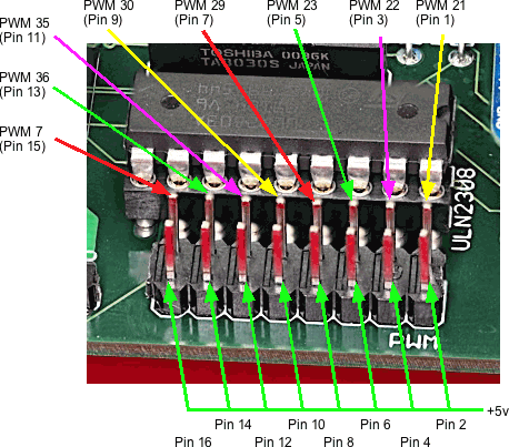
Note that the even-numbered pins connect to the +5v supply. The UNL2308 darlington array sinks current, it does not source current. You connect the +5v signal to your device and then connect your device's ground to the corresponding PWM output pin (one of the odd-numbered pins on the PWM header). When you program the corresponding PWM output pin with a '1', this opens a connection between the header pin and ground, thus providing a current path for your device. When an output pin is programmed with a '0' the darlington array is in a high-impedance ("open") state and no current flows -- the device is off.
Each pin can sink up to 500 mA. In theory, if you needed more than this you could solder two ULN2308 devices together. In practice, if you're sinking 500 mA on eight pins that corresponds to 4 amps flowing through the board. The board (particularly the power supply connector) probably won't be able to handle this. Furthermore, the traces leading from the ULN2308 to the header aren't especially big (probably around 25 mils) so they will get quite hot if you run too much current through them. Probably a limit of 100 mA/pin would be a good choice (drive a relay or motor controller if you need more current than this).
You can produce PWM waveforms out the Weensy 3.6 PWM pins using the Arduino analogWrite function. Be sure to program the Weensy 3.6 PWM pins as outputs before using the analogWrite function to produce PWM waveforms; i.e., include the following statements in your setup function.
    // PWM output lines -- always outputs:

    pinMode( pwm7, OUTPUT );
    pinMode( pwm21, OUTPUT );
    pinMode( pwm22, OUTPUT );
    pinMode( pwm23, OUTPUT );
    pinMode( pwm29, OUTPUT );
    pinMode( pwm30, OUTPUT );
    pinMode( pwm35, OUTPUT );
    pinMode( pwm36, OUTPUT );
The pwm7...pwm36 symbols have the following definitions:
#define pwm7        7
#define pwm21       21
#define pwm22       22
#define pwm23       23
#define pwm29       29
#define pwm30       30
#define pwm35       35
#define pwm36       36
I2C I/O on the Weensy 3.6
The Weensy 3.6 provides three independent I2C busses: one 3.3v I2C bus (I2C #0) on the Feather connectors (pins 11 & 12 on JP4 -- SCL0/SDA0), I2C bus #1 on its own header, and I2C #3 on its own header. Note that the I2C #2 bus is not available - the pins associated with that I2C bus on the Teensy 3.6 use alternate functions.
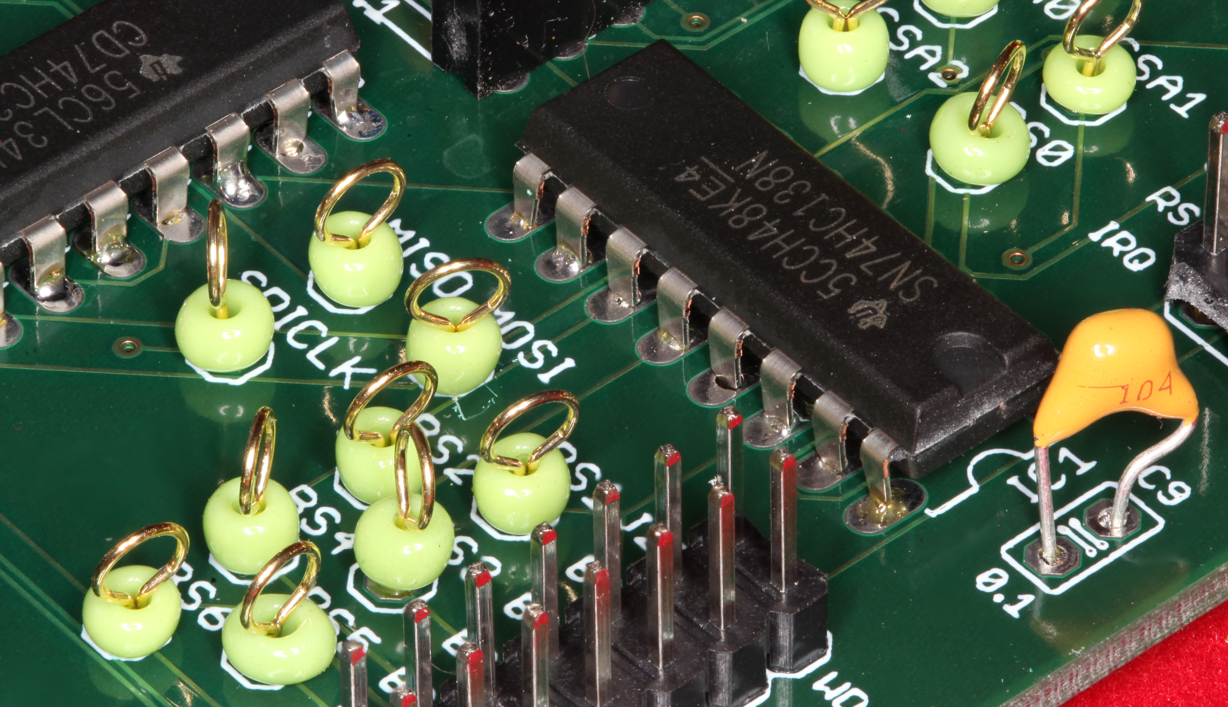
I2C bus #1 and I2C bus #3 operate using 5v logic (via an Adafruit BSS138 4-channel bi-directional level shifter). I2C1 an undedicated I2C bus present on the I2C1 header with the following pinout:
| Pin | Function |
|---|---|
| 1 | SCL1 - I2C clock line |
| 2 | SDA1 - I2C data line |
| 3 | VCC - 5V |
| 4 | Gnd |
High-resolution image shot with a Canon EOS 5D MII
I2C bus #3 has an identical pinout to I2C bus #1:
| Pin | Function |
|---|---|
| 1 | SCL3 - I2C clock line |
| 2 | SDA3 - I2C data line |
| 3 | VCC - 5V |
| 4 | Gnd |
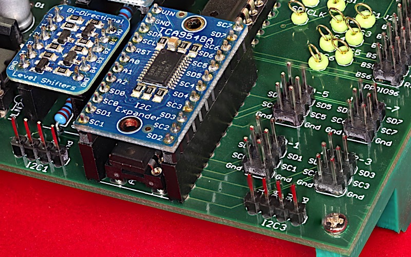
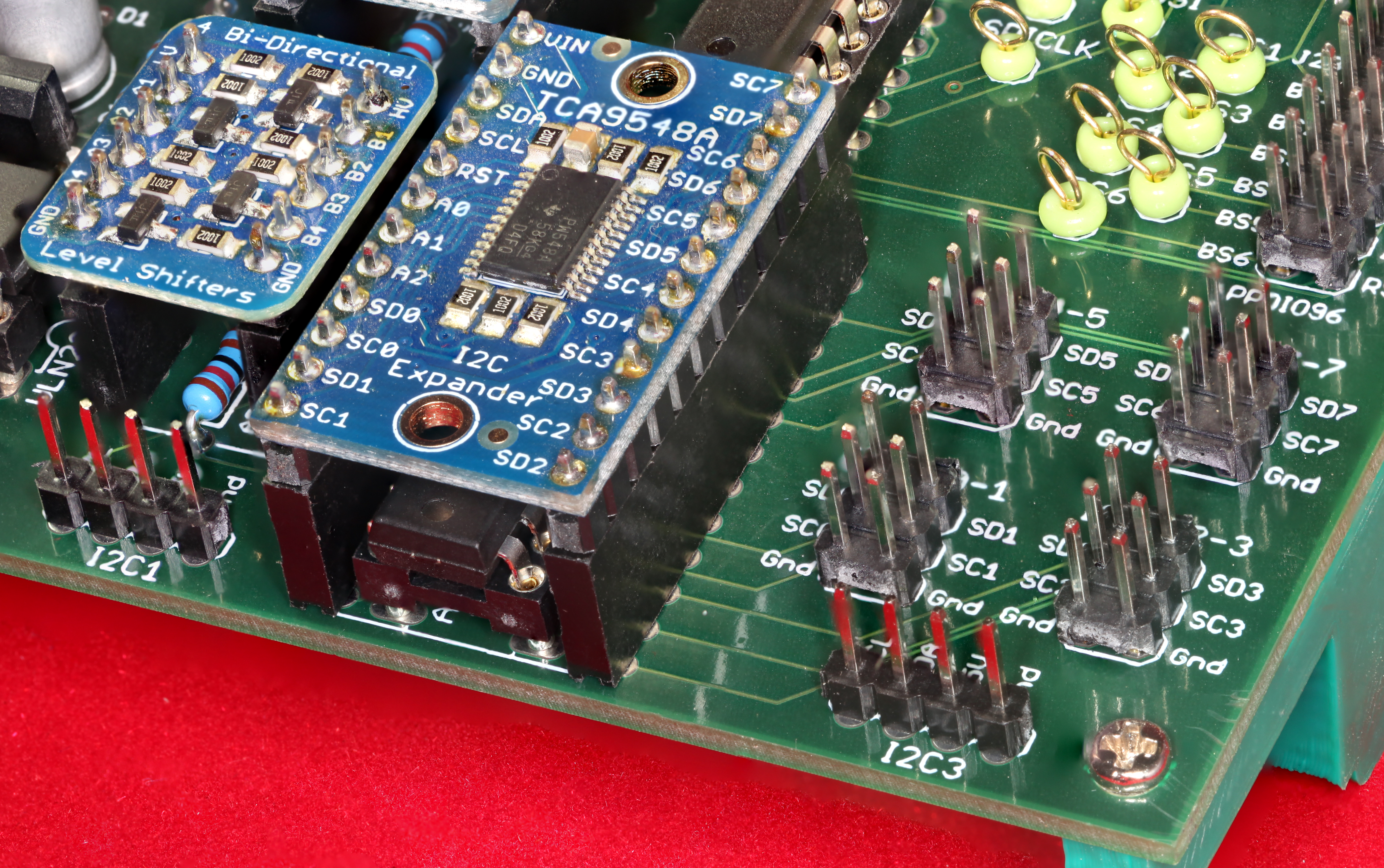
I2C3 reserves several addresses in the I2C address space to support Plantation Production's DAQ modules (specifically, the PPAIO-16/4 board). First of all, the Weensy 3.6 contains an Adafruit TCA9548A I2C expander board that expands I2C3 to eight I2C busses via multiplexing. The TCA9548A IC reserves I2C address 0x70. Writing a bit mask to this I2C address activates the eight additional I2C busses.
#define I2C_Multiplexer_Address 0x70

#define I2C_Port_0 1
#define I2C_Port_1 2
#define I2C_Port_2 4
#define I2C_Port_3 8
#define I2C_Port_4 0x10
#define I2C_Port_5 0x20
#define I2C_Port_6 0x40
#define I2C_Port_7 0x80

void setup()
{
		.
        .
        .
    Wire3.begin();

    // Set I2C port 0 (bit 0 = 1):

    writeTCA9548( I2C_Port_0 );
    	.
        .
        .

}

// Use I2C to write a byte to the specified register on address 0x70
//
//  Note: port 0-7 is selected by setting bit "port" to 1 in argument.

void writeTCA9548( uint8_t port )
{
    Wire3.beginTransmission( I2C_Multiplexer_Address );
    Wire3.send( port );
    Wire3.endTransmission();
}
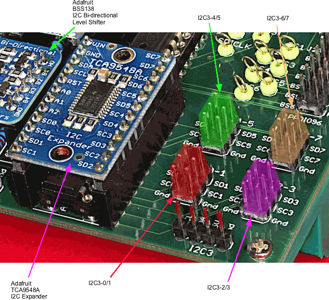
The expanded I2C busses appear on four 2x6 headers. Each of these four headers contains pins for two I2C busses. The pinout for each header is as follows:
| Pin | Function |
|---|---|
| 1 | SD0, SD2, SD4, or SD6 |
| 2 | SD1, SD3, SD5, or SD7 |
| 3 | SC0, SC2, SC4, or SC6 |
| 4 | SC1, SC3, SC5, or SC7 |
| 5 | Gnd |
| 6 | Gnd |
The 2x6 header pinout is compatible with the Plantation Productions' PPAIO-16/4 analog I/O board (16 channels of analog input and four channels of analog output).
Note that the TCA9548A I2C multiplexer only sends clock signals (SC0, SC1, ..., SC7) to the currently active I2C bus (I2C3-0, I2C3-1, ..., I2C3-7) as selected by writing the bit mask to the multiplexer IC. The I2C3 header is connected to the I2C3 bus before the multiplexer, so the clock and data pins on this header are always active, regardless of multiplexer bus selection. Connecting an I2C device to the I2C3 header makes that device active on all expanded I2C busses. Note that any device connected to the I2C3 header should not use I2C addresses 0x70 (used by the TCA9548A IC), addresses 0x60-0x63 (used by the DACs on the PPAIO-16/4 analog I/O board), or addresses 0x48-0x4b (used by the ADCs on the PPAIO-16/4 analog I/O board). This assumes, of course, that you want to reserve the ability to add one or more PPAIO-16/4 boards to your Weensy 3.6.
If you are interested in programming a PPAIO-16/4 board attached to a Weensy 3.6, here is some sample code that demonstrates reading and writing the ADCs and DACs:
SPI I/O on the Weensy 3.6
The Weensy 3.6 supports two independent SPI busses: SPI0 and SPI2.
SPI0 is a 3.3v SPI bus found on the Feather header (JP3):
- SCK0: Pin 6
- MOSI0: Pin 5
- MISO0: Pin 4
The chip select is hardware/software dependent. Typically the Featherwing will use one of the digital I/O lines (D3, D4, D5, D6, D8, D9, or D10) or one of the analog input lines (A0, A1, A2, A3, or A6 -- reprogrammed as outputs). Note that the A1 line's alternate function is CS0 (chip select SPI bus zero) so this is a common pin to use for SPI select.
The Weensy 3.6 uses the Teensy 3.6 SPI2 bus as the main SPI bus. The main SPI bus operates at 5V (through an Adafruit TXB0108 bi-directional level shifter) and connects to the PPDIO96 and PPDO headers on the Weensy 3.6.
High-resolution image shot with a Canon EOS 5D MII
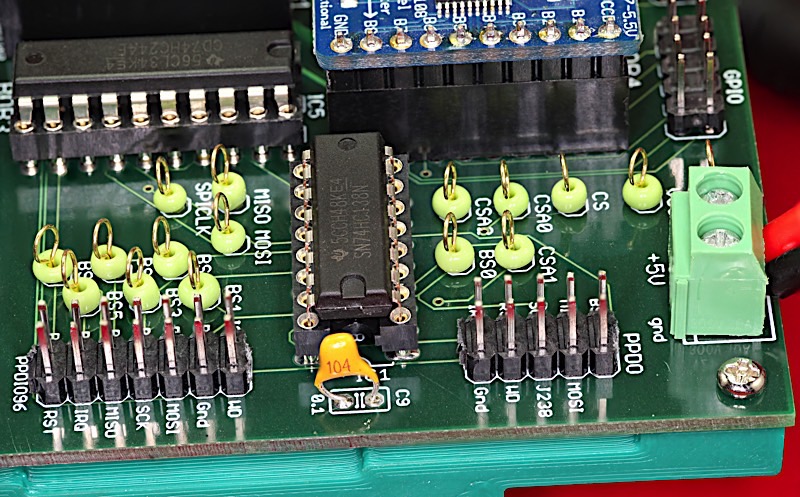
The Weensy 3.6 board provides SPI chip select expansion using an 74HC138 1-to-8 decoder along with four lines from the Teensy 3.2:
- CS2 (Teensy pin 43) drives the G2A enable line (active low) on the 74HC138
- CSA0 (Teensy pin 50) drives the "A" input/address pin on the 74HC138
- CSA1 (Teensy pin 49) drives the "B" input/address pin on the 74HC138
- CSA2 (Teensy pin 48) drives the "C" input/address pin on the 74HC138
Prior to any activity on the main SPI (2) bus, you must program pins 48, 49, and 50 with an appropriate chip select value (0-7). Here is some sample C++ code that demonstrates how to program the SPI (2) bus:
#define SPICS       43
#define CSA2        48
#define CSA1        49
#define CSA0        50


// In the setup function:
		.
        .
        .

    // SPI chip select lines -- always outputs:

    pinMode( SPICS, OUTPUT );
    pinMode( CSA0, OUTPUT );
    pinMode( CSA1, OUTPUT );
    pinMode( CSA2, OUTPUT );
    digitalWrite( SPICS, 1 );
    digitalWrite( CSA0, 0 );
    digitalWrite( CSA1, 0 );
    digitalWrite( CSA2, 0 );
    .
    .
    .

// Example that writes 32 bits of data to chip select zero:

	  digitalWrite( CSA0, 0 );	// Set A, B, C to 0, 0, 0
	  digitalWrite( CSA1, 0 );
	  digitalWrite( CSA2, 0 );

      SPI2.beginTransaction( WeensySPI );
      digitalWrite( SPICS, 0 );

      // Only writing, incoming data is ignored:

      SPI2.transfer( 0xff);
      SPI2.transfer( 0xff ;
      SPI2.transfer( 0xff);
      SPI2.transfer( 0xff);

      digitalWrite( SPICS, 1 );
      SPI2.endTransaction();
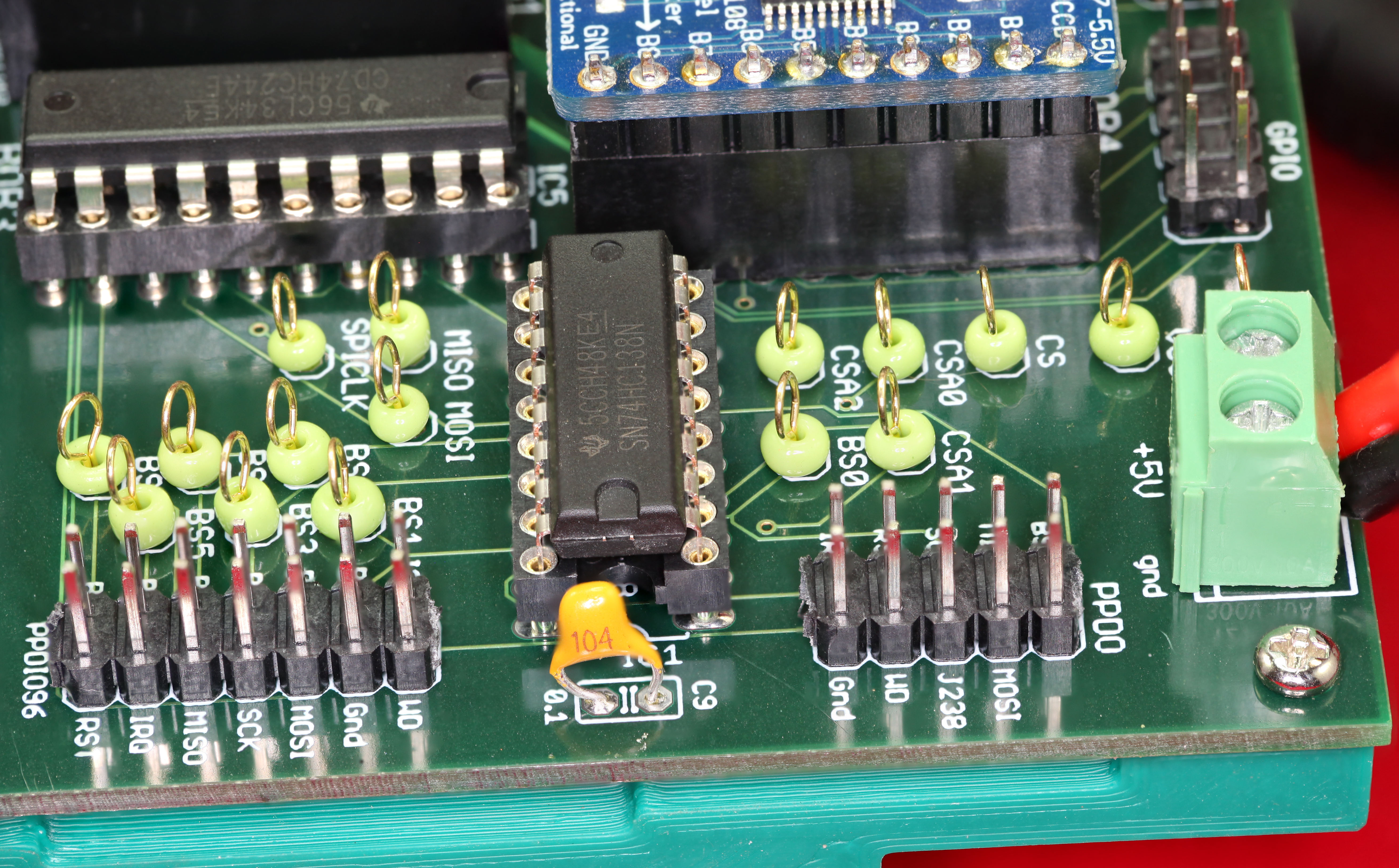
The Weensy 3.6 allocates the eight chip-select addresses as follows:
Chip Select 0 (BS0):
Connected to the "BS0" (board select zero) pin on the PPDO connector. Common practice is to treat devices connected to the PPDO connector as a serial shift register containing "n" bits (typically less than 160 bits, or 10 PPRelay-12 or PPSSR-16 boards).
Chip Selects 1-6 (BS1-BS6):
Connected to pins 1, 3, 5, 7, 9, 11, and 13 on the PPDIO96 connector on the Weensy 3.6. The PPDIO96 connector is an SPI bus with six chip selects capable of supporting up to six PPDIO96 boards (or other SPI peripherals).
Chip Select 7 (BS7):
Connected to the MCP23S17 SPI GPIO expanders on the Weensy 3.6 board.
The PPDIO96 (digital I/O) bus is a 14-pin connector. It has the following pinout:
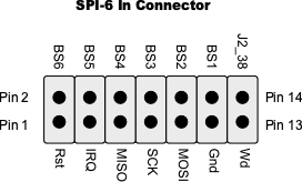
BS1..BS6 are six of the chip/board select signals from the 74HC138 decoder chip on the Weensy 3.6 board. When daisy-chaining PPDIO96 boards, these board select lines allow the selection of up to six PPDIO96 boards in the daisy chain (one board select line for each board).
MISO, MOSI, and SCK are the standard SPI bus signals (the fourth SPI signal, CS, is handled by BS1..BS6).
IRQ is an input to the Weensy 3.6board from the PPDIO96 boards. When activated for a particular MCP23S17 I/O expander chip, the PPDIO96 board(s) will assert this signal (active low) when requesting interrupt service. Note that you will have to program your own interrupt service routine to process this signal, if you activate it. The IRQ signal is connected to pin 53 on the Teensy 3.6 CPU board.
The J2_38 pin is reserved for end-user use. As such, the PPDIO96 boards ignore this signal line. If you create your own circuit designs to use the PPDIO96 bus, you can use this signal for whatever purpose you desire. J2_38 is connected to pin 47 on the Teensy 3.6 CPU board.
The WD signal is active (low) whenever the watchdog timer has timed out.
When the Weensy 3.6 board pulls the RST line line, this resets the MCP23S17 to their power-on state. This includes setting all I/O pins to inputs and disabling all internal pull-up resistors. For complete details on the MCP23S17 (power-on) reset state, please see the data sheet:
The PPDO (digital output) bus is a 10-pin connector. It has the following pinout:
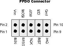
Note that the PPDO bus is an instance of the Weensy 3.6 SPI bus with a single chip/board select line (BS0). The PPDO bus presumes that there is a single shift register device hooked up to it (e.g., PPRelay-12 or PPSSR-16 boards). The size (in bits) of the shift register is arbitrary. In the Weensy system, each PPRelay-12 or PPSSR-16 board you daisy chain to the PPDO connector adds 16 bits to the size of the shift register. For example, if you have two PPRelay-12 and one PPSSR-16 boards daisy-chained to the PPDO connection, the shift register length is 48 bits (16 bits per board).
Assembling the Weensy 3.6 Board
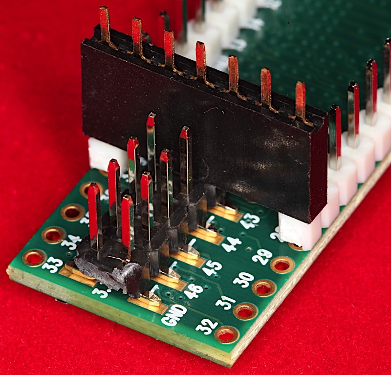
Perhaps the hardest part of building a Weensy 3.6 board is finding the 2.54mm pitch two-row SMT/SMD male headers. The Teensy 3.6 requires a 5x2 SMT male header, a 4x2 SMT male header, and a 3x2 SMT male header to provide access to the extra I/O pins present only on pads on the bottom of the Teensy 3.6:
High-resolution image shot with a Canon EOS 5D MII
High-resolution image shot with a Canon EOS 5D MII
The first step, before doing anything else, is to cut the trace between the VUSB pads on the bottom of the Teensy 3.6. The Weensy 3.6 will supply the 3.3v to power the Teensy, not the USB port. Cutting this trace prevents power supply conflicts between the Weensy 3.6 and the Teensy 3.6 USB port:
The next step is to create a jig that will hold the SMT headers in place while soldering them to the bottom of the Teensy 3.6. I used a pair of 1xn male headers and a 1x7 female header to hold the 2x5 SMT header in place while soldering it to the Teensy:
High-resolution image shot with a Canon EOS 5D MII
Solder only two pins on the header. Then move the jig down to the next set of pads and solder (only two pins) that header to the board. Finally, move the jig to the last set of pads and solder (only two pins) that header to the board. The result should look like this:
High-resolution image shot with a Canon EOS 5D MII
Before soldering down the remaining pins, carefully insert the Teensy 3.6 into the corresponding holes on the Weensy 3.6 and verify that the pins are all lined up properly. If a header has problems inserting into the Weensy board, unsolder the two pins for that header, realign and resolder it, and verify that the new position matches the Weensy board. Once you can easily insert the Teensy 3.6 onto the Weensy 3.6 board, solder the remaining pins to the bottom of the Teensy 3.6.
Once the three SMT headers are in place, put a 1x5 header into the five holes between the 5x2 and 3x2 SMT headers. Insert the Teensy 3.6 into the Weensy board (before soldering the 1x5 header in place). Verify the Teensy 3.6 is sitting snug on the Weensy board. Solder the five pins to the Teensy 3.6. DO NOT SOLDER THE PINS ONTO THE WEENSY BOARD YET! You are using the Weensy as a jig to hold the pins in place, you are not yet attaching the Teensy to the Weensy board.
Take two 1x5 headers. One one of the headers, remove pin #4. Insert the headers onto the Teensy 3.6 as shown here:
High-resolution image shot with a Canon EOS 5D MII
Before soldering the 1x5 headers to the Teensy, insert the Teensy onto the Weensy board and verify all the pins line up. With the Teensy still attached to the Weensy, solder the two 1x5 headers (total nine pins) to the Teensy. DO NOT SOLDER THE PINS ONTO THE WEENSY BOARD YET! You are using the Weensy as a jig to hold the pins in place, you are not yet attaching the Teensy to the Weensy board.
Remove the Teensy from the Weensy board. Insert two 24x1 headers onto the Weensy board, long pins into the Weensy (corresponding to the outside pins on the Teensy 3.6). Insert the Teensy 3.6 back onto the Weensy with the two 24x1 header pins poking through on the outside pins of the Teensy. Press firmly down on the Teensy to set it properly in the pins on the Weensy. Solder the pins poking through on the top of the Teensy 3.6. At this point, your work should look like the following:
High-resolution image shot with a Canon EOS 5D MII
Note that the Teensy is not yet soldered to the Weensy board. Now would be the time to do that. Solder a row of pins, trim the excess off, then move to the next row of pins.
Note: technically, you should pull the Teensy off the Weensy and solder it on last. This can help prevent damage to the part from electro-static discharge and other issues. The choice is your's. However, it's much easier to solder the Teensy on now (while it's plugged into the board) rather than later on after all the other parts are installed.
Why not socket the Teensy?
Given the cost of the Teensy 3.6 module (around $30 US), you might wonder if it would be a good idea to socket the Teensy so that it can be easily installed or removed. The problem with that theory is that sockets turn out to be one of the biggest failure points in an electronic circuit. If you really need to remove the Teensy 3.6 from the Weensy board (because of damage to the board), use a hot-air gun (or, better yet, a reflow work station) to heat the pins on the bottom of the Weensy board until the solder melts. Then you can easily remove the Teensy from the Weensy board.
Wiring up Passives and Transistors
Once the Teensy is installed on the Weensy board, the next step is to install all the small components (resistors, diodes, capacitors, LEDs, and transistors).
Wiring up resistors is relatively easy. They're not polarized so the only thing you have to do is verify that you're putting the correct resistor in each hole. If you have a good case of OCD (obsessive-compulsive disorder), you might want to always place the resistors in the holes such that the resistance color bars are read left-to-right or top-to-bottom. This makes it easier to read the resistor values once the resistors are all soldered in place.
R1 is a special case. This resistor (along with capacitor C4) provides the time constant for the watchdog timer. Nominally, this is a 100 kΩ resistor which, when coupled with a 47 µF capaciator, provides a fixed 4.7 second timeout period. If you want to use a different time constant, simply change the value of this resistor. The resistance, time 0.000047 specifies the time constant. So, for example, if you would prefer about a 10-second time (9.8 seconds, actually), just substitute a 200 kΩ resistor. Conversely, if you'd like a 2.35-second timeout, substitute a 50 kΩ resistor.
Weensy 3.6 Rev 4 and later boards (the pictures in this tutorial are all from a Rev 1 board, so the picture below doesn't show this) provide a set of holes for a potentiometer overlaid on the R1 resistor pads. These pads allow you to install a BI 67W R100K (or R200K) potentiometer so you can field-adjust the timeout period.
The 0.1 µF and 10 µF capacitors are not polarized and may be placed on the board without regard to the lead position. The 47 µF capacitor is an electrolytic capacitor and is polarized. There is a small "-" sign above the hole into which you must insert the negative lead.

High-resolution image shot with a Canon EOS 5D MII
Note: although the board says that this is a 50 µF capacitor, the actual value is 47 µF. 50 µF is the ideal value (50 µF * 100 kΩ = 5 seconds), 47 µF is the value you can actually buy. The negative lead on the electrolytic capacitor is the shorter lead. There is usually a marking on the capacitor as well. Here's a picture of a 47 µF capacitor installed on the board:
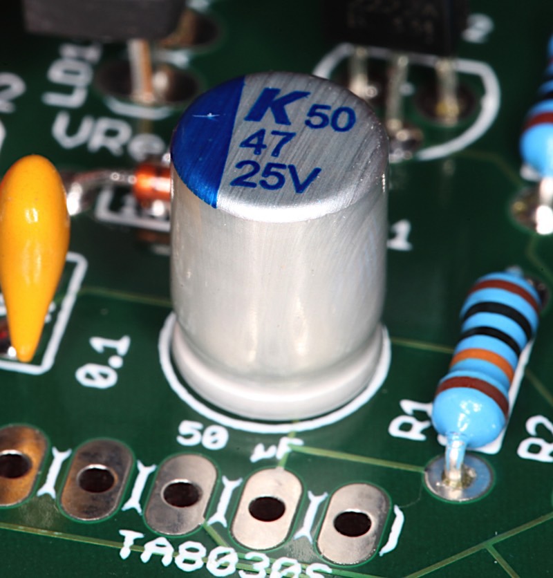
High-resolution image shot with a Canon EOS 5D MII
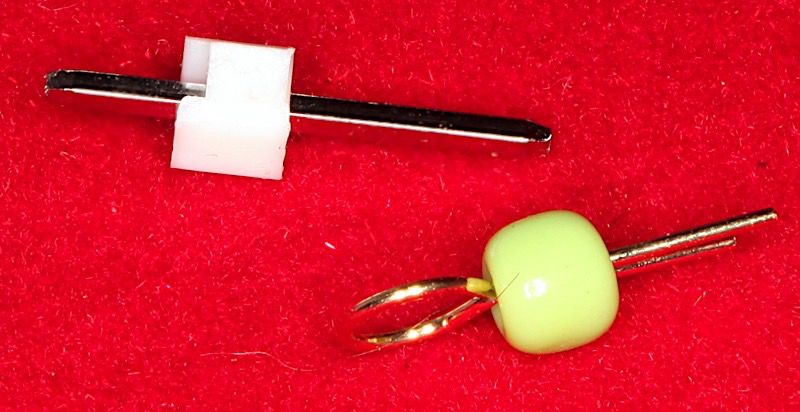
Wiring up LEDs and Transistors
LEDs and transistors on the Weensy 3.6 represents a special (and painful) case. Not only are these devices polarized, but it is also the case that different variants of these devices switch leads and other identifying markings. Therefore, you should always test each device before soldering it onto the Weensy 3.6 board and, whatever you do, don't trust the markings on the circuit board or the device. There are two tools you should have when attaching LEDs and transistors to the Weensy 3.6: a DVM (specifically, an Ohm meter) and a transistor tester. Any DVM will do. I highly recommend the SainSmart 12864 LCR-T4 pocketable transistor tester:
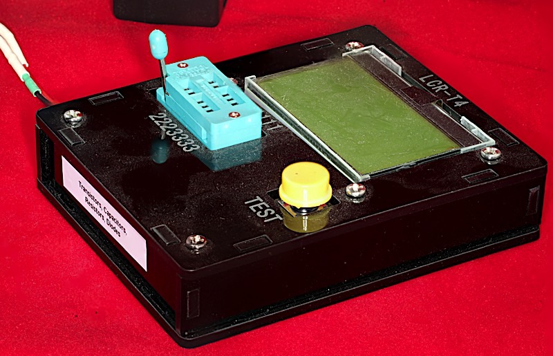
High-resolution image shot with a Canon EOS 5D MII
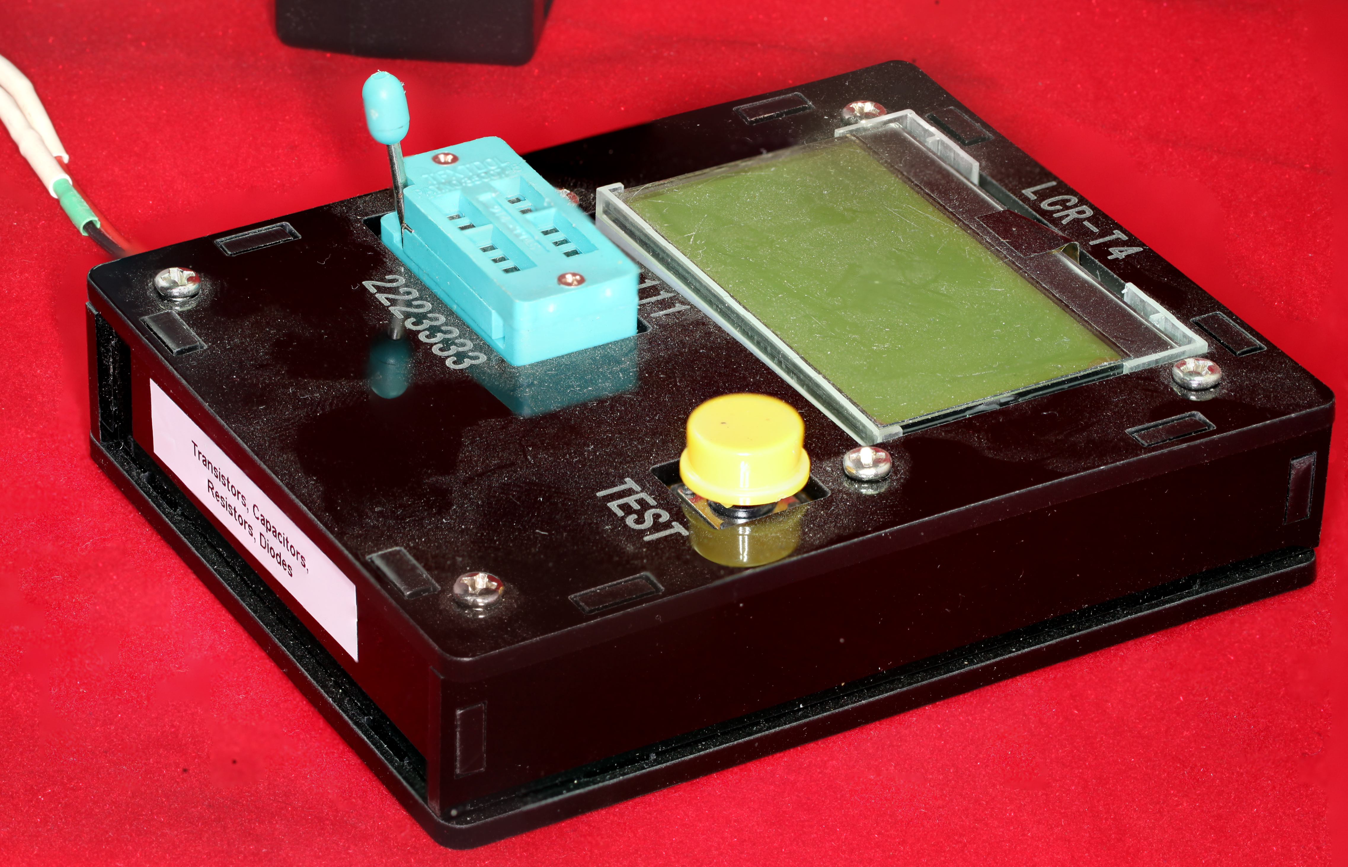
In addition to testing transistors (most kinds), the LCR-T4 will also test capacitors, resistors, diodes, triodes, triacs, and other devices. This is an amazing unit and I highly recommend it. The only negative to this unit is that it runs off a 9v battery and tends to chew through batteries at a rapid clip. I solved this problem by attaching a 9v wall wart to the unit. This unit is perfect for testing the 2N2222 transistors and LEDs found on the Weensy 3.6 board. You can easily find this device on Amazon. It's typically under $20.
When installing LEDs on the Weensy board note that the cathode ("-" terminal) is always the shorter of the two leads on the LED. Do NOT rely on the notch on the LED (matching up with the notch on the LED silkscreen on the Weensy). Usually the notch is associated with the cathode lead, but I've had some batches of LEDs from China where the notch on the LED was next to the anode ("+" terminal). I always stick my LEDs into the LCR-T4 to test them prior to soldering them onto a PCB. While there is never any ambiguity about which terminal is the cathode or anode (the cathode is always the shorter one), sticking the LED into the LCR-T4 also flashes the LED during testing so that I can verify that the LED actually works (yes, I have gotten several defective LEDs over the years). The LED notch markings on the Weensy 3.6 silk screen are always the cathode; insert the cathode (shorter pin) into the hole closest to this marking on the Weensy. Again, do not rely on the notch on the actual LED to mark the cathode -- use the shorter pin (and you can verify this with the LCR-T4.
The 2N2222 transistor comes in two varieties: 2N2222A (possibly other suffixes) and P2N2222A (possibly other suffixes). The difference between the two is that the 2N2222 has the emitter on pin 1 and the collector on pin 3 wherease the P2N2222 has the collector on pin 1 and the emitter on pin 3. Either version will work fine on the Weensy 3.6, you'll simply have to reverse the transistor when using one variety versus the other. As luck would have it, the generic 2N2222 part in the Eagle library that I used on the Weensy 3.6 board seems to have been the PN2222 variety, so if you're using the standard 2N2222 part, you'll have to reverse the leads (with respect to the notch on the silk screen markings). This issue has been resolved. Newer versions of the board (e.g., Rev 5 and beyond) use a different Eagle part which has the proper silkscreen markings. Note that the P2N2222 part has the pins organized in a triangular shape, the 2N2222 Eagle part has the pins arranged in a straight line.
I always begin by putting a transistor in the LCR-T4 transistor tester. This identifies which pin is the emitter (pin 1 or pin 3). Next, I use an DVM to determine which pin on the transisor pads on the Weensy is connected to ground. The emitter is always connected to ground. On Rev 2 of the Weensy 3.6 board, if the notch on the 2N2222 silkscreen is pointed down, the emitter is always the pin on the right. However, it's always a good idea to measure the resistance between that pin and a ground connection somewhere (e.g., the "Gnd" pin on the I2C3 header). You should measure a resistance of about an Ohm or less. On the board I'm building for this tutorial (an older board), all my 2N2222 transistors had to be mounted with the pins reversed (that is, the notch on the transistor package was opposite that of the silk screen markings). Newer boards won't have this issue.
![]()
High-resolution image shot with a Canon EOS 5D MII
Installing the Voltage Regulator
The LD1117v33 3.3v regulator converts the 5v supplied to the Weensy 3.6 to 3.3v as needed by the Teesny 3.6 and other components on the board. This 1A voltage regulator provides just enough current for the Teensy 3.6 and the Feather bus (assuming the Featherwings don't consume too much power). Install the voltage regulator with the back of the regulator closest to the Teensy module:
High-resolution image shot with a Canon EOS 5D MII
Installing ICs
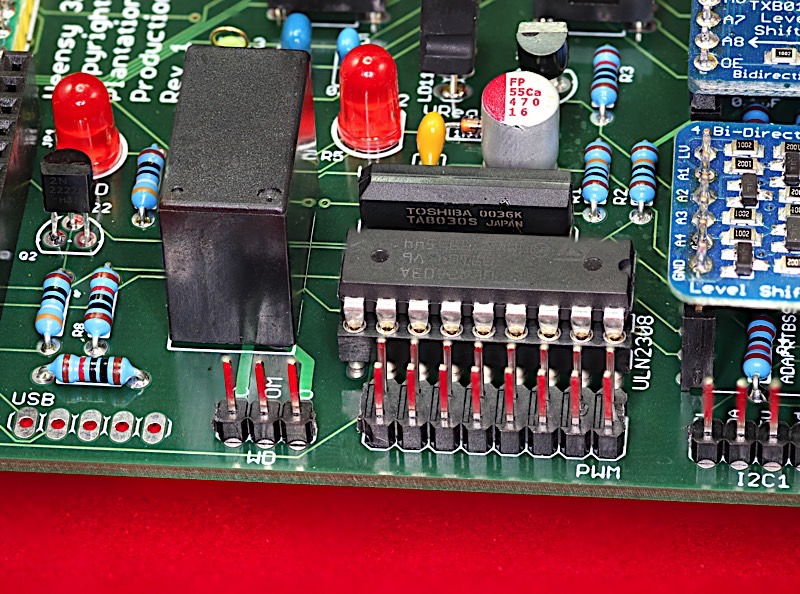
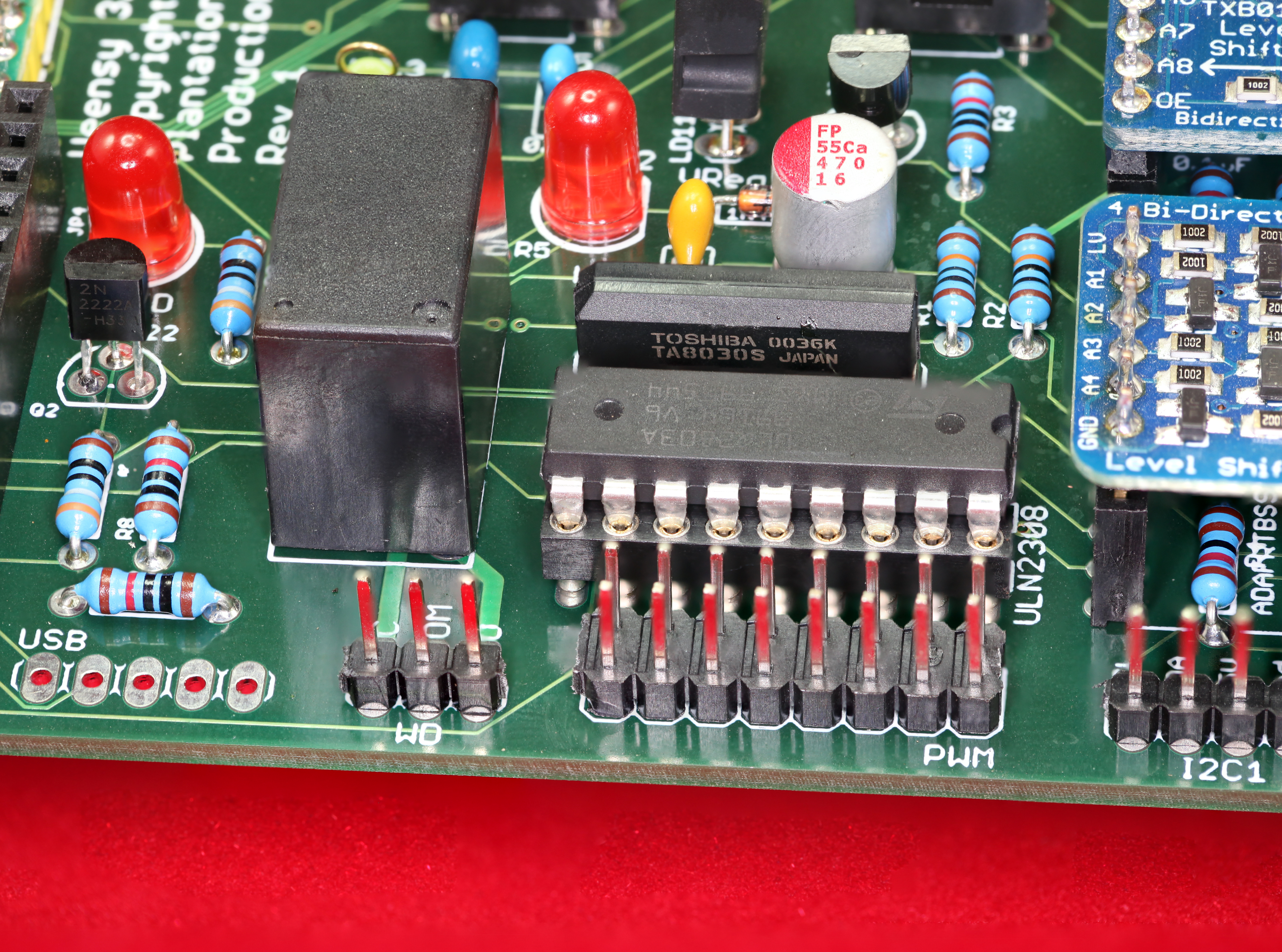
Next, install the TA8030S, ULN2308, 74HC74, 74HC244, 74HC138 and MCP23S16 integrated circuits onto the Weensy 3.6 PCB. Although the DIP switch is not technically an IC, it's most appropriate to install the DIP switch along with the other ICs.
As noted for the Teensy 3.6, you can use sockets for many of these ICs if you're paranoid; just keep in mind that the sockets are more likely to fail than the ICs, so socketing the ICs make create more problems than it solves. Note that the 74HC74 flip-flop mounts underneath the TCA9548A breakout board. Therefore, there may not be sufficient room to socket the 74HC74. If you want to socket this IC, you should verify that it will fit underneath the TCA0548A before actually soldering the socket in place.
High-resolution image shot with a Canon EOS 5D MII
Installing the Adafruit Breakout Boards
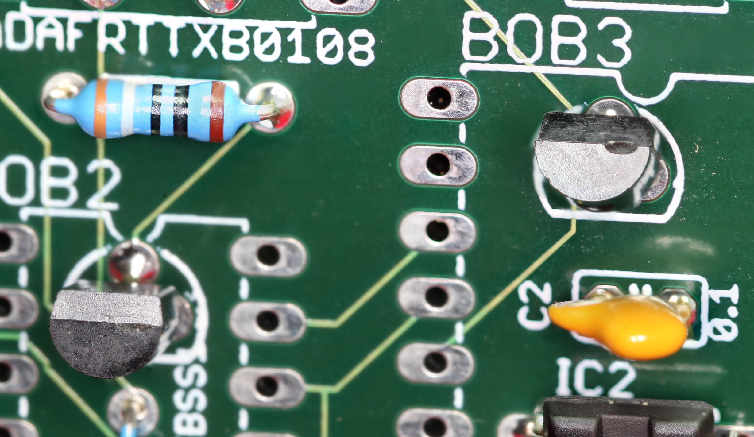
The next step is to install the female headers onto which you'll plug the Adafruit TXB0108 bi-directional level shifters (2), the Adafruit BSS138 bi-directional level shifter, and the Adafruit TCA9548A I2C multiplexer. In theory, you could solder these headers directly to the Weensy 3.6 PCB. In practice, it's safer to mount these headers on the actual breakout boards (BoBs) and use the BoBs as jigs so that you know you're soldering the headers properly in place (so that it is easy to install or remove the BoBs):
High-resolution image shot with a Canon EOS 5D MII
In theory, you could solder the BoBs directly onto the Weensy 3.6. However, there are parts mounted underneath the BoBs, so you may not have enough clearance to do this.
You can also install a 10x1 female header for the Sparkfun MAX3232 BoB. This is an optional item. If you aren't intending to use the DB-9 RS232 connection you can skip installing this header. Note that, because this is a 10x1 header, you don't really need to install the header on the MAX3232 BoB prior to soldering it onto the board. Also, if you intend to use the DB-9 RS232 connection exclusively (that is, you're not going to ever use the FTDI serial connection), you can skip installing the header and solder the MAX3232 BoB directly onto the Weensy 3.6.
If you do intend to use the DB-9 RS-232 connection, now would be a good time to install the DB9M connector onto the Weensy 3.6 PCB.

High-resolution image shot with a Canon EOS 5D MII
Don't forget to install the 16x1 and 12x1 headers for the Adafruit Feather bus (they are adjacent to the Teensy 3.6 module). When installing the Feather headers, it's a good idea to plug them into a Featherwing device (using the Featherwing as a jig) to ensure proper alignment. In the following picture, I've used an Adafruit Ethernet Featherwing as my jig:
High-resolution image shot with a Canon EOS 5D MII
Installing the Header Pins on the Weensy 3.6
Now is a good time to install all the male header pins on the Weensy 3.6. Some of the headers are optional depending on your use case; they are:
- FTDI (RS-232 to USB) header. No need to install this if you're not use RS-232 serial or you're exclusively using the MAX3232 and DB-9 RS-232 connection. Note: the FTDI cable and the MAX3232 are mutually exclusive. You cannot install both in the system; they will interfere with one another and may damage one another (or even the Teensy 3.6).
- Debug header -- only install if you intend to use the Debug signals on the Teensy 3.6.
- USB header -- only install if you intend to use the USB Host features on the Teensy 3.6.
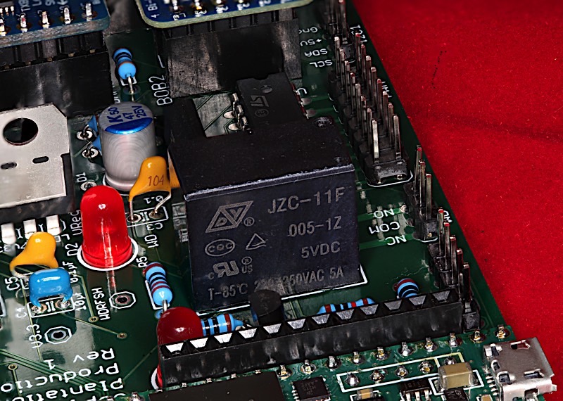
Installing the Relay on the Weensy 3.6
Now install the relay on the Weensy 3.6 board. The relay is a JZC-11F-05VDC-1Z relay available from Sparkfun. The relay is rated for up to 5A at 30V, though you should limit it to about 1A because of PCB trace limitations.
High-resolution image shot with a Canon EOS 5D MII
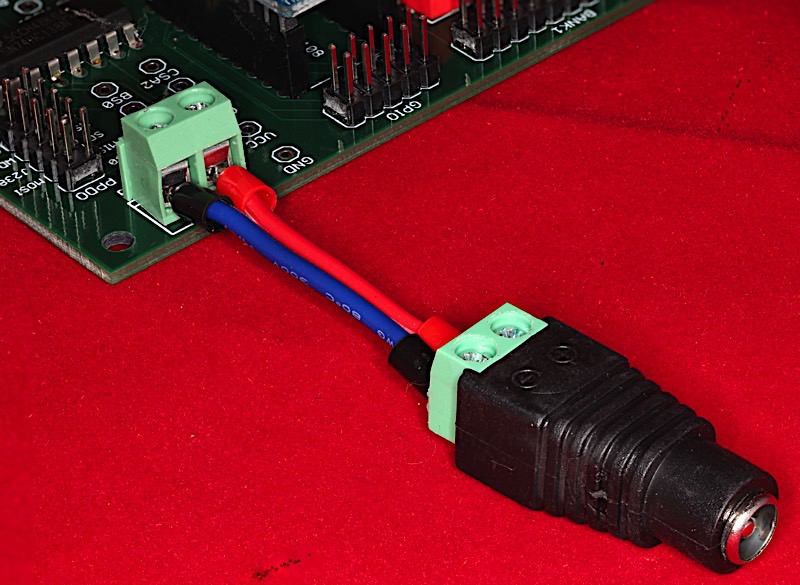
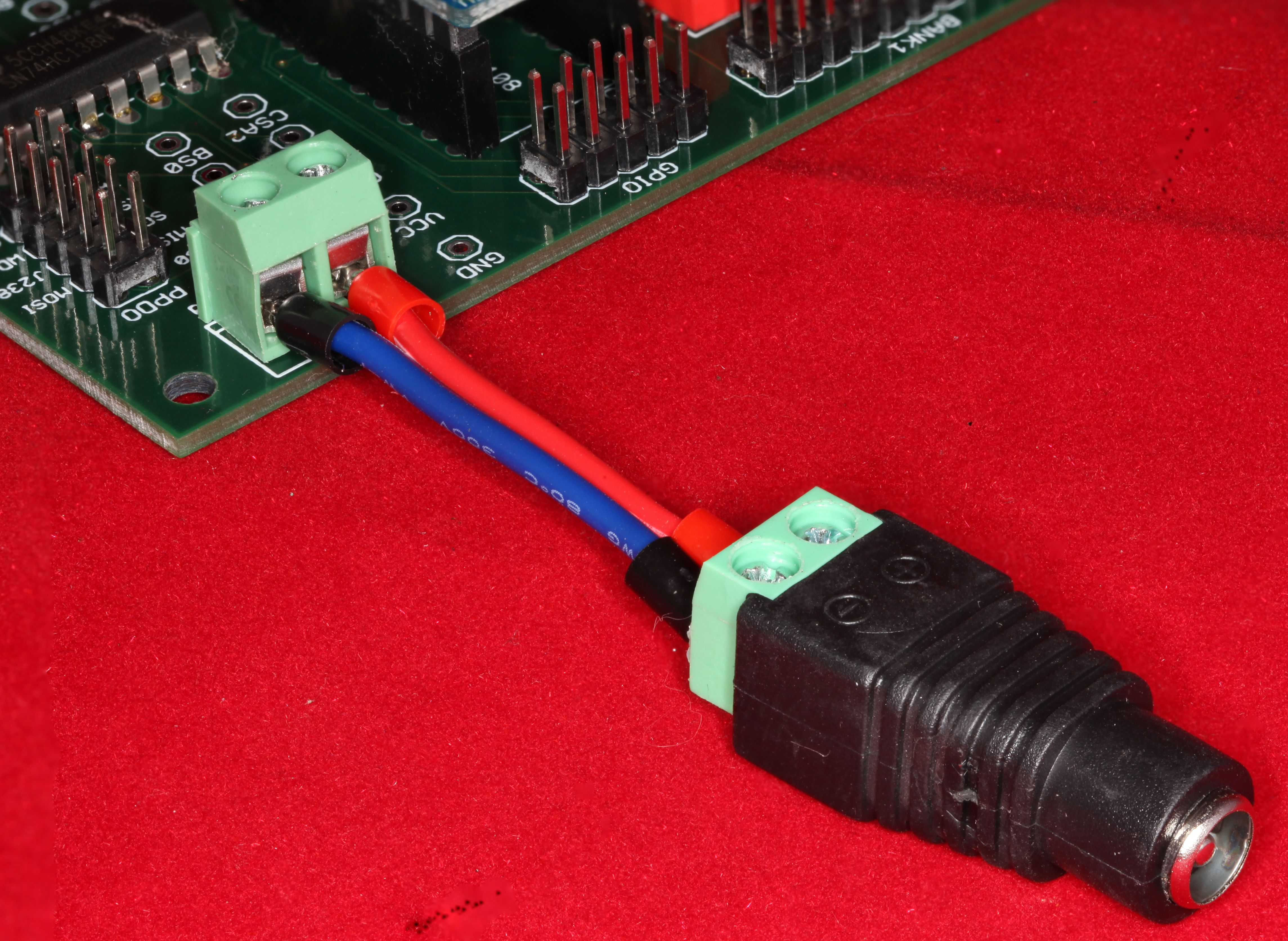
Installing the Power Terminal
Now install the two-pin screw terminal for the power supply. I recommend at least a 5V 4A power supply for the Weensy 3.6. Adafruit has a 5V 4A power supply that is perfect for the job. If you use the Adafruit power supply, you'll also need a 2.1mm female power jack adapter and a couple wires to go between the adapter and the Weensy 3.6 board. I recommend 18 AWG wire with ferrules (you can find ferrules and their crimping tool on Amazon).
High-resolution image shot with a Canon EOS 5D MII
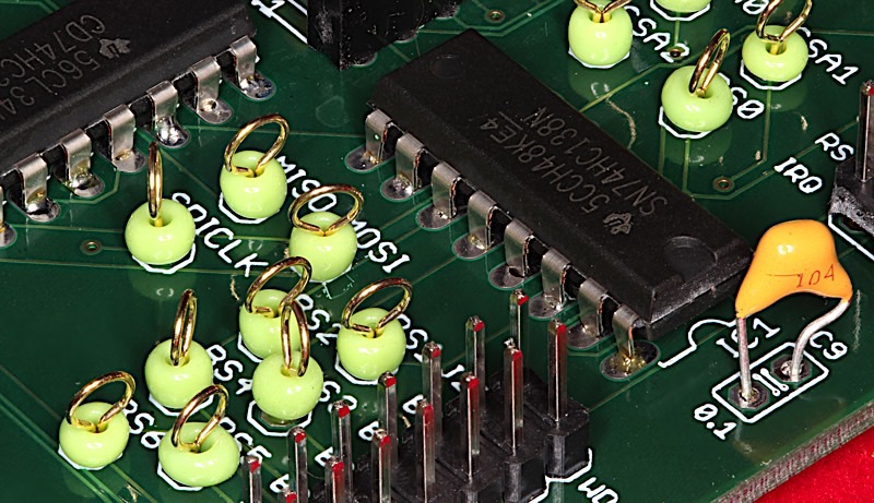
Optional: Installing the Test Pins
The Weensy 3.6 board includes several test points on the board. These test points are useful for testing the hardware; they're also useful for testing software as they provide access to important signal points (to which you can attach the probes of a DVM, oscilloscope, or logic analyzer). You can either purchase "official" test pins or create your own by cutting off a single pin from a strip of 1xn header pins. The advantage of the "official" test pins is that it is often easier to clip a scope or logic analyzer probe onto the loop of a test pin.
Note that installing test pins is strictly optional. Even if you don't install them, the pads are still preset on the Weensy PCB so you can still touch a probe to the pad and measure the signal. The test pins have the advantage that you can clip a probe on them and operate hands-free thereafter. Here's a picture showing several of the test pins installed:
High-resolution image shot with a Canon EOS 5D MII
One Last Assembly Item
Before calling it quits, it's a real good idea to inspect each and every pin you've soldered on the Weensy 3.6 board. It's very easy to miss a few pins here and there (I missed about four pins when creating this tutorial). Much easier to fix this problem by inspection rather than trying to debug why the circuit isn't working later on...
Now that you've finished assembling the board, it's a good idea to spray some flux remover over all the solder joints and clean off the solder flux (mostly on the bottom of the board, but there are a few points on the top, such as the Teensy 3.6 module, that also have soldered joints with excess solder flux floating around).
For What It's Worth...
The pictures in this assembly tutorial were shot using a Rev 1 version of the Weensy 3.6. The current revision is Rev 5. There are a couple functional differences between Rev 1 and Rev 2 that an astute eye might catch. First of all, the zener diode (1N4728A) and 27 Ω resistor are not present on the Rev 1 board (I soldered them between pins 8 and 13 on the 74HC74 IC underneath the board; see the schematic for details). A second difference, which you can see by looking at the board layout image earlier on this web page, is that the smaller capacitors (0.1 µF and 10 µF have three holes rather than two. This is because capacitors with these values come in many different sizes. By having three holes (with two of them connected together) it is possible to accomodate capacitors from many different manufactures without having to bend any legs way back (as is evident in the preceding picture). I've also added several new test pins, a pullup resistor (on the IRQ line), and made a couple changes to the circuit. Someday I might get around to shooting new images, but with focus stacking I have to shoot about 40 pictures for each image and merge them all together, so it takes about a half an hour for each image. Given the number of pictures in this tutorial, that's a low priority item. To be honest, I can't image that the older images will be a stumbling block for anyone.
Testing the Weensy 3.6 Board
After you've soldered the last component onto the board, I'm sure you're itching to try it out. Sadly, chances are pretty good there are some mistakes made during assembly. Now comes the boring part -- testing your work to ensure that the board is working properly.
The Smoke Test
The very first test is the "smoke" test. This involves applying power to the Weensy board and verifying that it doesn't make a popping sound and doesn't produce a cloud of smoke as the unit self-destructs.
Seriously, though, when you apply power the "Pwr" LED should illuminate and if you've got a stock Teensy 3.6 module installed, the LED on the Teensy should be blinking on and off. The watchdog LED (and relay) may be doing funny things every 5 seconds or so, ignore that for now.
If the Pwr LED does not illuminate and the Teensy 3.6 LED is not blinking, test the 3.3V test point with a DVM (3.3V and Gnd should read around 3.3v). If not, verify that the regulator is the proper one and it's installed properly and isn't hot (warning: if you install it backwards it can get very hot very quickly).
If the Teensy LED is blinking but the Pwr LED is not, chances are you've installed the Pwr LED backwards (or it is defective, you did test it, right?). If the Pwr LED is lit and you've got 3.3V, but the Teensy LED is not blinking, either your Teensy isn't working properly or it doesn't have the stock "BLINK" sketch installed. Check all the solder connections on the bottom of the Weensy board (to the Teensy) and verify that there aren't any shorts.
Programming the Teensy
Before going any further, you did cut the VUSB jumper, right? If not, it's still possible to do it (though a lot more difficult as the pads are barely accessible between the Teensy and the Weensy PCBs). You don't want to plug in a USB cable to the Teensy and power the Weensy board unless the jumper is cut (see the beginning of the assembly tutorial for more details). We'll start with the Weensy version of the "BLINK" program. The Weensy utility LED (also known as the "heartbeat" LED) is attached to pin 2. The following code is a modification of the standard Arduino BLINK sketch that toggles pin 2 rather than pin 13. This version also contains code to reset the watchdog latch on power up and refresh it every couple of seconds to avoid having the watchdog LED light up.
/*
  Blink
  Turns on an LED on for one second, then off for one second, repeatedly.

  This example code is in the public domain.
 */

// Pin 13 has an LED connected on most Arduino boards.
// Pin 11 has the LED on Teensy 2.0
// Pin 6  has the LED on Teensy++ 2.0
// Pin 13 has the LED on Teensy 3.0
// Pin 2 is the Heartbeat LED on the Weensy board
// give it a name:
int led = 2;


#define wd_rfsh     52
#define Reset       51


// Must send a positive pulse to the TA8030s
// to refresh the watchdog timer:

void watchdogRefresh( void )
{
    digitalWrite( wd_rfsh, 1 );
    delay( 1 );
    digitalWrite( wd_rfsh, 0 );
}

// Must send a negative-going pulse to the DS1834
// chip to cause a reset. The pulse must be at least
// 350 msec wide.

void toggleReset( void )
{
        digitalWrite( Reset, 0 );
        delay( 350 );
        digitalWrite( Reset, 1 );
}

// the setup routine runs once when you press reset:
void setup()
{
    // initialize the digital pin as an output.
    pinMode(led, OUTPUT);

    // Stuff needed by the watchdog timer:

    pinMode( Reset, OUTPUT );
    pinMode( wd_rfsh, OUTPUT );
    toggleReset();
    delay( 350 );       // Must have 350 msec delay after reset.
    watchdogRefresh();          // Must do this at least once every 4 seconds

}

// the loop routine runs over and over again forever:
void loop()
{
    digitalWrite(led, HIGH);    // turn the LED on (HIGH is the voltage level)
    delay(1000);                // wait for a second
    digitalWrite(led, LOW);     // turn the LED off by making the voltage LOW
    delay(1000);                // wait for a second
    watchdogRefresh();          // Must do this at least once every 4 seconds
}
Note: pin 13 on the Teensy 3.6 will control the Teensy 3.6's on-board LED. However, the Adafruit Feather bus also uses this pin for the SPI clock output so you shouldn't use this pin as an LED control if you're using the SPI features on the Feather bus.
Testing the Watchdog Timer
The following sketch starts by resetting (and refreshing) the watchdog timer. Then it allows the watchdog timer to expire and verifies that the watchdog latch remains open. Finally, it verifies that after the watchdog is reset, it will expire again if it is not refreshed.
/*
  WatchdogTest (Weensy 3.6 version)
  Verifies the proper operation of the Weensy 3.6 watchdog timer

  This example code is in the public domain.
 */

#define wd_rfsh     52
#define Reset       51
#define wd_latch    54

unsigned long   startTimer;
unsigned long   curTimer;
unsigned        latch;
int             latchFailure    = false;
int             wdFailure       = false;
int             testDone        = false;


// Must send a positive pulse to the TA8030s
// to refresh the watchdog timer:

void watchdogRefresh( void )
{
    digitalWrite( wd_rfsh, 1 );
    delay( 1 );
    digitalWrite( wd_rfsh, 0 );
}

// Must send a negative-going pulse to the DS1834
// chip to cause a reset. The pulse must be at least
// 350 msec wide.

void toggleReset( void )
{
        digitalWrite( Reset, 0 );
        delay( 350 );
        digitalWrite( Reset, 1 );
}

// the setup routine runs once when you press reset:

void setup()
{

    Serial.begin( 9600 );

    // Stuff needed by the watchdog timer:

    pinMode( Reset, OUTPUT );       // Reset pin is an output.
    pinMode( wd_rfsh, OUTPUT );     // Watchdog refresh is an output.
    pinMode( wd_latch, INPUT );    // Read watchdog state here.

    delay( 1000 );
    Serial.println( "Watchdog test program" );

    watchdogRefresh();              // Guarantee that the WD is refreshed
    toggleReset();                  // Reset watchdog timer latch.
    delay(500);                     // Give relay time to open, etc.
    toggleReset();                  // Reset watchdog timer latch.
    delay(500);                     // Give relay time to open, etc.
    watchdogRefresh();              // Guarantee that the WD is refreshed
    delay( 100 );
    latch = !digitalRead( wd_latch );
    if( latch )
    {
        Serial.println( "WD Latch failed to clear after reset/refresh" );
        latchFailure = true;
    }
    startTimer = millis();          // Time at start of timeout period

}

// the loop routine runs over and over again forever:

void loop()
{
    curTimer = (millis() - startTimer);
    if(  curTimer == 6000 && digitalRead( wd_latch ) && !wdFailure)
    {
        Serial.println( "Watchdog timer failed to expire" );
        wdFailure = true;
    }
    if( curTimer == 6001 && !digitalRead( wd_latch ) )
    {
        toggleReset();
        delay( 350 );
        if( !digitalRead( wd_latch ))
        {
            Serial.println( "Failed to reset watchdog timer" );
        }
    }
    if( curTimer >= 10000 && !testDone )
    {
        if( !digitalRead( wd_latch ))
        {
            Serial.println( "Watchdog timer failed to expire, again" );
        }
        Serial.println( "Watchdog test complete" );
        testDone = true;
    }

}
Testing thePWM/ULN2308 Outputs
The following sketch starts by resetting (and refreshing) the watchdog timer. Then it allows the watchdog timer to expire and verifies that the watchdog latch remains open. Finally, it verifies that after the watchdog is reset, it will expire again if it is not refreshed. To test the output pins, you'll need to wire up the following simple circuit:
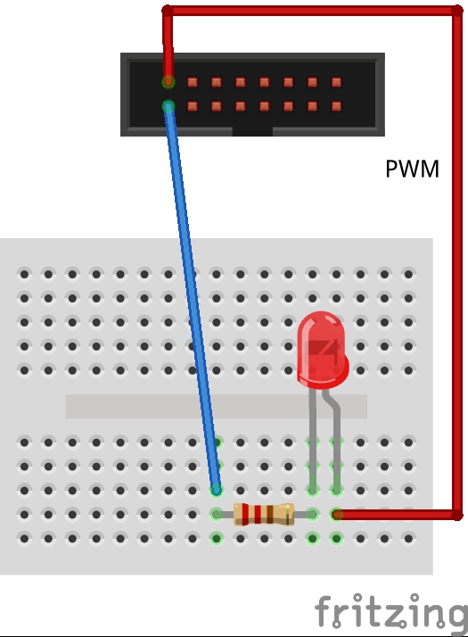
The resistor is a 220 Ω resistor. The LED can be any typical LED; the cathode (negative/short) terminal is the one with the bent pin in the diagram. Connect the resistor directly to one of the bottom pins (closest to the edge of the Weensy PCB) of the PWM connector (the bottom pins are all connected to +5v, so it doesn't matter which one you connect it to). Connect the cathode of the LED to one of the top pins in the diagram, as follows:
| Pin | Function | Note |
|---|---|---|
| 15 | PWM 7 | Top pin on left (connection in diagram) |
| 13 | PWM 36 | |
| 11 | PWM 35 | |
| 9 | PWM 30 | |
| 7 | PWM 29 | |
| 5 | PWM 23 | |
| 3 | PWM 22 | |
| 1 | PWM 21 | Top pin on right |
The following program will start by blinking all the PWM outputs for five seconds. After that, it presents a menu with eight selections ('a' through 'h') allowing you to pick a specific channel to test. In the Arduino IDE serial window, select the input text edit box, type a single character ('a' through 'h') and press the "send" button. This will send out a varying PWM signal (from dim to full brightness) over a couple seconds to allow you to verify that PWM operation is happening. When you select a particular PWM channel, an LED hooked up to that output should vary from dim to bright.
Note that pressing any character other than 'a' through 'f' (which must be lower case) will turn off all PWM channels.
If you've hooked up a single LED (as shown in the earlier Fritzing diagram), you can test the individual channels by moving the wire connected to the LED across each of the top pins on the connector (as documented in the above table).
/*
  PWMTest (Weensy 3.6 version)
  Verifies the proper operation of the Weensy 3.6 PWM Circuitry

  This example code is in the public domain.
 */

#define pwm7        7
#define pwm21       21
#define pwm22       22
#define pwm23       23
#define pwm29       29
#define pwm30       30
#define pwm35       35
#define pwm36       36

#define wd_rfsh     52
#define Reset       51
#define wd_latch    54

char            inputCh = ' ';
unsigned long   pwmCntr = 0;
unsigned        pwmPin  = 0;


// Must send a positive pulse to the TA8030s
// to refresh the watchdog timer:

void watchdogRefresh( void )
{
    digitalWrite( wd_rfsh, 1 );
    delay( 1 );
    digitalWrite( wd_rfsh, 0 );
}

// Must send a negative-going pulse to the DS1834
// chip to cause a reset. The pulse must be at least
// 350 msec wide.

void toggleReset( void )
{
        digitalWrite( Reset, 0 );
        delay( 350 );
        digitalWrite( Reset, 1 );
}

// Turn off all the PWM outputs:

void clearAll( void )
{
        digitalWrite( pwm7,  0 );
        digitalWrite( pwm21, 0 );
        digitalWrite( pwm22, 0 );
        digitalWrite( pwm23, 0 );
        digitalWrite( pwm29, 0 );
        digitalWrite( pwm30, 0 );
        digitalWrite( pwm35, 0 );
        digitalWrite( pwm36, 0 );
}


// the setup routine runs once when you press reset:

void setup()
{
    Serial.begin( 9600 );
    delay( 1000 );
    Serial.println( "PWM Test Program" );


    // Stuff needed by the watchdog timer:

    pinMode( Reset, OUTPUT );       // Reset pin is an output.
    pinMode( wd_rfsh, OUTPUT );     // Watchdog refresh is an output.
    pinMode( wd_latch, INPUT );    // Read watchdog state here.


    // PWM output lines -- always outputs:

    pinMode( pwm7, OUTPUT );
    pinMode( pwm21, OUTPUT );
    pinMode( pwm22, OUTPUT );
    pinMode( pwm23, OUTPUT );
    pinMode( pwm29, OUTPUT );
    pinMode( pwm30, OUTPUT );
    pinMode( pwm35, OUTPUT );
    pinMode( pwm36, OUTPUT );


    watchdogRefresh();              // Guarantee that the WD is refreshed
    toggleReset();                  // Reset watchdog timer latch.
    delay( 350 );
    watchdogRefresh();              // Guarantee that the WD is refreshed

    // For a couple seconds on startup, blink all the PWM outputs:

    for( int i=0; i < 5; ++i )
    {
        digitalWrite( pwm7,  1 );
        digitalWrite( pwm21, 1 );
        digitalWrite( pwm22, 1 );
        digitalWrite( pwm23, 1 );
        digitalWrite( pwm29, 1 );
        digitalWrite( pwm30, 1 );
        digitalWrite( pwm35, 1 );
        digitalWrite( pwm36, 1 );
        delay( 500 );
        clearAll();
        delay( 500 );
        watchdogRefresh();

    }
    Serial.println();
    Serial.println( "Choose item:" );
    Serial.println();
    Serial.println( "a.  PWM 7  (pin 15 -- leftmost pin)" );
    Serial.println( "b.  PWM 36 (pin 13)" );
    Serial.println( "c.  PWM 35 (pin 11)" );
    Serial.println( "d.  PWM 30 (pin  9)" );
    Serial.println( "e.  PWM 29 (pin  7)" );
    Serial.println( "f.  PWM 23 (pin  5)" );
    Serial.println( "g.  PWM 22 (pin  3)" );
    Serial.println( "h.  PWM 21 (pin  1 -- rightmost pin)" );
    Serial.println( "anything else turns off all pins" );

}

// the loop routine runs over and over again forever:

void loop()
{
    ++pwmCntr;
    if( Serial.available() > 0 )
    {
        inputCh = Serial.read();
        analogWrite( pwm7,  0 );
        analogWrite( pwm21, 0 );
        analogWrite( pwm22, 0 );
        analogWrite( pwm23, 0 );
        analogWrite( pwm29, 0 );
        analogWrite( pwm30, 0 );
        analogWrite( pwm35, 0 );
        analogWrite( pwm36, 0 );
        switch( inputCh )
        {
            case 'a':
                pwmPin = pwm7;
                break;

            case 'b':
                pwmPin = pwm36;
                break;

            case 'c':
                pwmPin = pwm35;
                break;

            case 'd':
                pwmPin = pwm30;
                break;

            case 'e':
                pwmPin = pwm29;
                break;

            case 'f':
                pwmPin = pwm23;
                break;

            case 'g':
                pwmPin = pwm22;
                break;

            case 'h':
                pwmPin = pwm21;
                break;

            case 0xa:
            case 0xd:
                break;

            default:
                clearAll();
                pwmPin = 0;
                break;
        }
    }
    watchdogRefresh();
    if( pwmPin != 0 )
    {
        analogWrite( pwmPin, (pwmCntr/8) & 0xff );
    }
}
Testing the I2C Busses
To test the I2C busses, I wired up an Adafruit 4725 DAC breakout board to each of the I2C busses (I2C1, I2C3, and I2C3-0...I2C3-7).
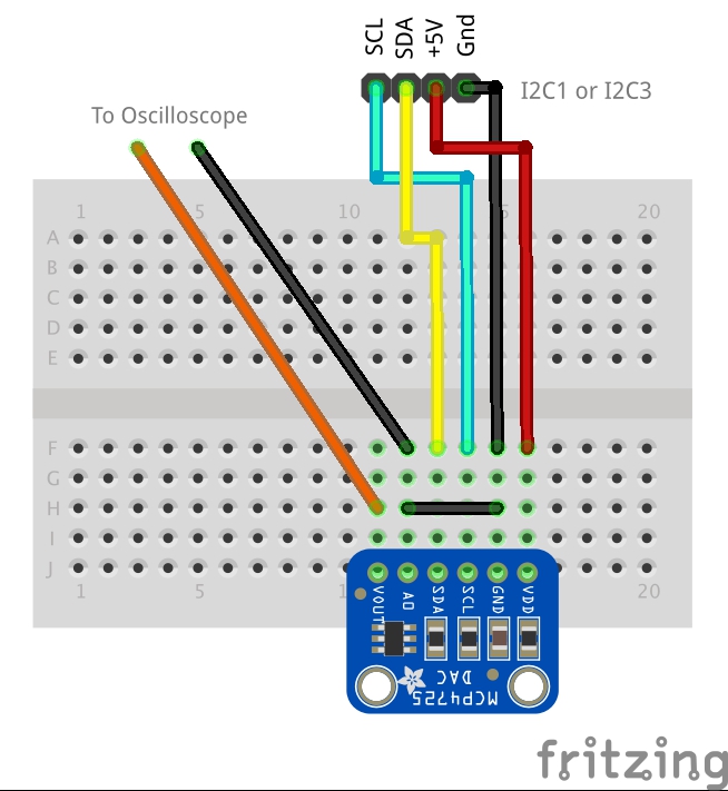
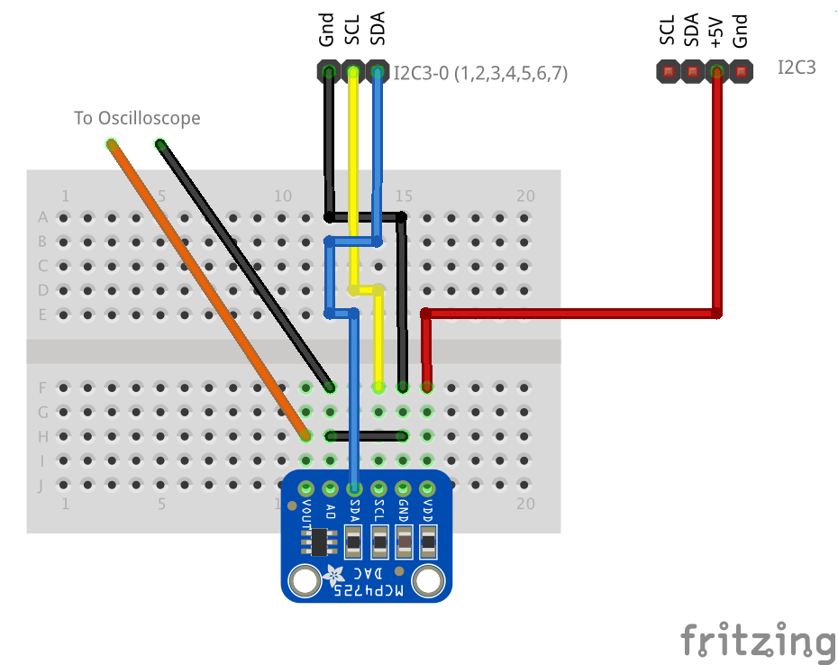
For the test code, I used the Adafruit MCP4725 library and the triangle wave example program (slightly modified to use Teensy's Wire library). Note that you mus change the "whichBus" constant at the beginning of this code to match the particular I2C bus you are testing:
| whichBus | I2C Bus (Header) Selected |
|---|---|
| 1 | I2C1 |
| 3 | I2C3 |
| 30 | I2C3-0 |
| 31 | I2C3-1 |
| 32 | I2C3-2 |
| 33 | I2C3-3 |
| 34 | I2C3-4 |
| 35 | I2C3-5 |
| 36 | I2C3-6 |
| 37 | I2C3-7 |
/**************************************************************************/
/*!
    @file     trianglewave.pde
    @author   Adafruit Industries
    @license  BSD (see license.txt)

    This example will generate a triangle wave with the MCP4725 DAC.

    This is an example sketch for the Adafruit MCP4725 breakout board
    ----> http://www.adafruit.com/products/935

    Adafruit invests time and resources providing this open source code,
    please support Adafruit and open-source hardware by purchasing
    products from Adafruit!
*/
/**************************************************************************/


#include

// Set whichBus to one of the following values:
//
//  1:  I2C1
//  3:  I2C3 (I2C3 header)
//  30: I2C3-0
//  31: I2C3-1
//  32: I2C3-2
//  33: I2C3-3
//  34: I2C3-4
//  35: I2C3-5
//  36: I2C3-6
//  37: I2C3-7

#define whichBus 1

#if whichBus == 1

    #define testBus Wire1
    #define i2c3Bus 0

#elif whichBus == 3

    #define testBus Wire3
    #define i2c3Bus 0

#elif whichBus == 30

    #define testBus Wire3
    #define i2c3Bus 1

#elif whichBus == 31

    #define testBus Wire3
    #define i2c3Bus 2

#elif whichBus == 32

    #define testBus Wire3
    #define i2c3Bus 4

#elif whichBus == 33

    #define testBus Wire3
    #define i2c3Bus 8

#elif whichBus == 34

    #define testBus Wire3
    #define i2c3Bus 0x10

#elif whichBus == 35

    #define testBus Wire3
    #define i2c3Bus 0x20

#elif whichBus == 36

    #define testBus Wire3
    #define i2c3Bus 0x40

#elif whichBus == 37

    #define testBus Wire3
    #define i2c3Bus 0x80

#else

    #error Illegal I2C bus selected
    #define testBus Wire1
    #define i2c3Bus 0

#endif


#define I2C_Multiplexer_Address 0x70
#define LEDPin      2
#define Reset       51
#define wd_rfsh     52


// writeTCA9548
//
//  Selects specified I2C expansion bus on I2C3.
//
// Use I2C (Wire3) to write a byte to the specified register on address 0x70
//
//  Note: port 0-7 is selected by setting bit "port" to 1 in argument.

void writeTCA9548( uint8_t port )
{
    Serial.println( port );
    Wire3.beginTransmission( I2C_Multiplexer_Address );
    Wire3.send( port );
    Wire3.endTransmission();
}

// Must send a positive pulse to the TA8030s
// to refresh the watchdog timer:

void watchdogRefresh( void )
{
    digitalWrite( wd_rfsh, 1 );
    digitalWrite( wd_rfsh, 0 );
}

// Must send a negative-going pulse to the DS1834
// chip to cause a reset. The pulse must be at least
// 350 msec wide.

void toggleReset( void )
{
        digitalWrite( Reset, 0 );
        delay( 350 );
        digitalWrite( Reset, 1 );
}

// From MCP4725.h:

#define MCP4726_CMD_WRITEDAC            (0x40)  // Writes data to the DAC
#define MCP4726_CMD_WRITEDACEEPROM      (0x60)  // Writes data to the DAC and the EEPROM (persisting the assigned value after reset)

class MCP4725
{
    public:
        MCP4725();
        void begin(uint8_t a);
        void setVoltage( uint16_t output, bool writeEEPROM );

    private:
        uint8_t _i2caddr;
};


// From MCP4725.cpp:

MCP4725::MCP4725()
{
}

void MCP4725::begin(uint8_t addr)
{
    _i2caddr = addr;
    testBus.begin();
}

/**************************************************************************/
/*!
    @brief  Sets the output voltage to a fraction of source vref.  (Value
            can be 0..4095)
    @param[in]  output
                The 12-bit value representing the relationship between
                the DAC's input voltage and its output voltage.
    @param[in]  writeEEPROM
                If this value is true, 'output' will also be written
                to the MCP4725's internal non-volatile memory, meaning
                that the DAC will retain the current voltage output
                after power-down or reset.
*/
/**************************************************************************/

void MCP4725::setVoltage( uint16_t output, bool writeEEPROM )
{
    // First, select the appropriate I2C3 bus.
    // Note: set i2c3Bus to 0 if writing to the I2C1 or I2C3 headers.

    #if( i2c3Bus != 0 )

        writeTCA9548( i2c3Bus );

    #endif

    testBus.beginTransmission(_i2caddr);
    if (writeEEPROM)
    {
        testBus.write(MCP4726_CMD_WRITEDACEEPROM);
    }
    else
    {
        testBus.write(MCP4726_CMD_WRITEDAC);
    }
    testBus.write(output / 16);                   // Upper data bits          (D11.D10.D9.D8.D7.D6.D5.D4)
    testBus.write((output % 16) << 4);            // Lower data bits          (D3.D2.D1.D0.x.x.x.x)
    testBus.endTransmission();

    // Deselect I2C3 bus when we are done:

    #if( i2c3Bus != 0 )

        writeTCA9548( 0 );

    #endif

}


// Test code to generate a triangle wave:

MCP4725 dac;

void setup(void)
{
    Serial.begin(9600);
    delay( 1000 );
    Serial.println("I2C Test program");

    pinMode( wd_rfsh, OUTPUT );
    pinMode( LEDPin, OUTPUT );
    pinMode( Reset, OUTPUT );

    watchdogRefresh();
    toggleReset();
    delay( 350 );
    watchdogRefresh();

    // Initialize the I2C output

    testBus.begin();
    testBus.setRate( F_BUS, 400000 );

    #if( whichBus >= 30 && whichBus <= 37 )

        writeTCA9548( 0 );

    #endif


    // For Adafruit MCP4725A1 the address is 0x62 (default) or 0x63 (ADDR pin tied to VCC)
    // For MCP4725A0 the address is 0x60 or 0x61
    // For MCP4725A2 the address is 0x64 or 0x65

    dac.begin(0x62);

    Serial.println("Generating a triangle wave");
}

void loop(void)
{
    uint32_t counter;

    // Run through the full 12-bit scale for a triangle wave

    digitalWrite( LEDPin, 0 );
    for (counter = 0; counter < 4095; counter++)
    {
        dac.setVoltage(counter, false);
    }
    watchdogRefresh();

    digitalWrite( LEDPin, 1 );
    for (counter = 4095; counter > 0; counter--)
    {
        dac.setVoltage(counter, false);
    }
    watchdogRefresh();
}
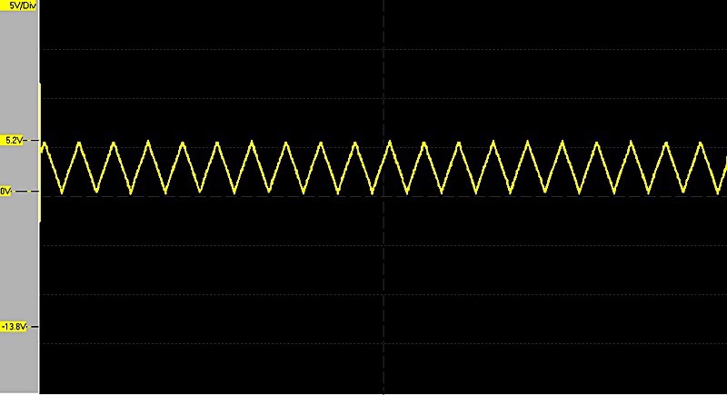
Here's the output I captured on my Oscilloscope:
Testing the SPI Busses
To test the SPI busses, I wired up an MCP23S17 GPIO expander IC on a small wireless breadboard. I chose this device because the Weensy 3.6 has two MCP23S17 ICs on it, so I could use the same test code for the on-board ICs as well as for testing the PPDIO and PPDO SPI busses. Here's the wiring diagram for the MCP23S17 (the diagram shows an MPC23017 because Frizting doesn't have an MCP23S17 - for our purposes, we'll treat this as an MCP23S17):
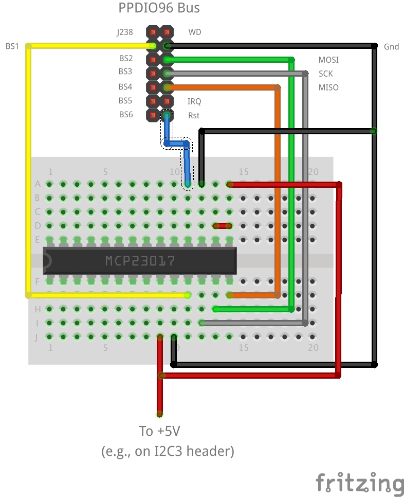
Note that the MCP23S17 address pins (A0=pin 15, A1=pin 16, and A2=pin 17) to +5V, +5V, and Gnd (respectively) so that this device has the address 3 (%011). Note that the on-board MCP23S17 ICs have hardwired addresses 1 (IC4) and 2 (IC3) so three was done just to make the software less confusing (the off-board MCP23S17 is on a separate chip select line, so it doesn't matter if it has the same hardware address as one of the other ICs; however, using different addresses helps make the code clearer). See the MCP23S17 Data Sheet for more details on chip selects and hardware address pins.
Once the off-board MCP23S17 is wired up, here's some code to test the SPI bus by accessing the off-board and on-board MCP23S17 ICs:
// SPITest.ino
//
//  Test code for the Weensy SPI bus.

#include


// Change whichBS to match the board select (BSn, n=0..6) connected to the MCP23S17 IC.
//
//  0:  BS0 on Weensy PPDO connector
//  1:  BS1 on Weensy PPDIO96 connector
//  2:  BS2 on Weensy PPDIO96 connector
//  3:  BS3 on Weensy PPDIO96 connector
//  4:  BS4 on Weensy PPDIO96 connector
//  5:  BS5 on Weensy PPDIO96 connector
//  6:  BS6 on Weensy PPDIO96 connector
//
//  Note: board select 7 (BS7) is the chip select for the two MCP23S17 ICs
//  found on the Weensy board. They are always tested along with the MCP23S17
//  associated with one of the above board (chip) selects.

#define whichBS         1

#define onChipBS        7

#define mcp23S17_aux    3
#define mcp23S17_IC3    2
#define mcp23S17_IC4    1


#define spics           43
#define mosi            44
#define miso            45
#define SCK             46

#define a2              48
#define a1              49
#define a0              50
#define Reset           51
#define wd_rfsh         52
#define wd_latch        54


#define MCP23S17_ADDRESS    0x40

// registers
#define MCP23S17_IODIRA 0x00
#define MCP23S17_IPOLA 0x02
#define MCP23S17_GPINTENA 0x04
#define MCP23S17_DEFVALA 0x06
#define MCP23S17_INTCONA 0x08
#define MCP23S17_IOCONA 0x0A
#define MCP23S17_GPPUA 0x0C
#define MCP23S17_INTFA 0x0E
#define MCP23S17_INTCAPA 0x10
#define MCP23S17_GPIOA 0x12
#define MCP23S17_OLATA 0x14


#define MCP23S17_IODIRB 0x01
#define MCP23S17_IPOLB 0x03
#define MCP23S17_GPINTENB 0x05
#define MCP23S17_DEFVALB 0x07
#define MCP23S17_INTCONB 0x09
#define MCP23S17_IOCONB 0x0B
#define MCP23S17_GPPUB 0x0D
#define MCP23S17_INTFB 0x0F
#define MCP23S17_INTCAPB 0x11
#define MCP23S17_GPIOB 0x13
#define MCP23S17_OLATB 0x15

#define MCP23S17_INT_ERR 255

SPISettings MCP23S17settings; //( 2000000, MSBFIRST, SPI_MODE1 );


uint8_t flip4[16] =
                {
                    0, 0x8, 0x4, 0xc,
                    0x2, 0xa, 0x6, 0xe,
                    0x1, 0x9, 0x5, 0xd,
                    0x3, 0xb, 0x7, 0xf
                };


// Must send a positive pulse to the TA8030s
// to refresh the watchdog timer:

void watchdogRefresh( void )
{
    digitalWrite( wd_rfsh, 1 );
    delayMicroseconds( 10 );
    digitalWrite( wd_rfsh, 0 );
    delayMicroseconds( 10 );
}

// Must send a negative-going pulse to the DS1834
// chip to cause a reset. The pulse must be at least
// 350 msec wide.

void toggleReset( void )
{
        digitalWrite( Reset, 0 );
        delay( 350 );
        digitalWrite( Reset, 1 );
}


// setBSAdrs writes the board select address (0..7) to
// the 74HC138 that generates the BS0..BS7 signals.

void setBSAdrs( int adrs )
{
    if( adrs <0 || adrs > 7 )
    {
        adrs = 0;
    }
    digitalWrite( a0, adrs & 1 );
    digitalWrite( a1, (adrs >> 1) & 1 );
    digitalWrite( a2, (adrs >> 2) & 1 );
    delayMicroseconds(1);
} // setBSAdrs


// SPI write register function:

void writeReg( uint8_t board, uint8_t chip, uint8_t regAddr, uint8_t regValue )
{
    if( board <= 7 && chip <= 7 )
    {
        SPI2.beginTransaction( MCP23S17settings );
        setBSAdrs( board );
        digitalWrite( spics, LOW );
        SPI2.transfer( MCP23S17_ADDRESS | (chip << 1));
        SPI2.transfer( regAddr );
        SPI2.transfer( regValue );
        digitalWrite( spics, HIGH );
        SPI2.endTransaction();
    }
}

// SPI read register function.
//
//  Note: the board argument is the chip select (BSn, n=0..7) value.
//  Chip is the MCP23s16 hardware address (0 for external MCP23S17 being
//  tested, 1 for IC4 on-board MCP23S17, and 2 for IC3 on-board MCP23S17).

void readReg( uint8_t board, uint8_t chip, uint8_t regAddr, uint8_t &result )
{
    if( board <= 7 && chip <= 7 )
    {
        SPI2.beginTransaction( MCP23S17settings );
        setBSAdrs( board );
        digitalWrite( spics, LOW );
        SPI2.transfer( MCP23S17_ADDRESS | (chip << 1) | 1);
        SPI2.transfer( regAddr );
        result  = SPI2.transfer( 0 );
        digitalWrite( spics, HIGH );
        SPI2.endTransaction();
    }
}

// readBank -
//
//  For banks 0 & 1, read the twelve bits associated with that bank and rearrange
//  the bits read in order to match the bit ordering on the connector (not a bit-
//  for-bit matching because of trace optimizations on the circuit board).
//
//  Bank 2 is only 8 bits and corresponds to the 8 dip switches.

uint16_t readBank(  uint8_t bank )
{
            uint8_t regA;
            uint8_t regB;

    switch( bank )
    {
        case 0:
            readReg( onChipBS, mcp23S17_IC4, MCP23S17_GPIOB, regB );
            readReg( onChipBS, mcp23S17_IC4, MCP23S17_GPIOA, regA );
            return
                    (flip4[ (regA & 0xf0) >> 4]) << 8
                |   regB;

        case 1:
            readReg( onChipBS, mcp23S17_IC4, MCP23S17_GPIOA, regA );
            readReg( onChipBS, mcp23S17_IC3, MCP23S17_GPIOB, regB );
            return
                    (flip4[ (regA & 0xf)])
                |   regB << 4;

        case 2:
            readReg( onChipBS, mcp23S17_IC3, MCP23S17_GPIOA, regA );
            return regA & 0xff;

    }
    return 0;

}


void initialize23S17( void )
{
    uint8_t r;

    // Initialize the off-board MCP23S17
    //
    //  Note ICON = 0x7c is
    //
    //  BANK    = 0     - No register banking, interleave/pair bank registers
    //  MIRROR  = 1     - INTB mirrors INTA
    //  SEQOP   = 1     - Increment address register after each access
    //  DISSLW  = 1     - Slew rate (I2C only)
    //  HAEN    = 1     - Hardware address enable
    //  ODR     = 1     - Open drain on INTA/INTB
    //  INTPOL  = 0     - Interrupt polarity
    //  Not used= 0


    // Initially, all MCP23S17 ICs respond to address 0. Write to
    // IOCON to set the HAEN bit. In theory, a single write should
    // affect *ALL* devices on a given chip select line (which is
    // why the following code contains two writes - on for the on-board
    // MCP23S17 ICs [onChipBS] and one for the MCP23S17 wired to PPDIO96
    // bus [whichBS]).
    //
    //  Side Note: due to a bug in the MCP23S17 chip, if there are more than
    // four MCP23S17 devices wired to the same chip select line, two
    // writes would be required: one at address zero and one at address four.
    // This issue doesn't apply here.


    writeReg( whichBS, 0, MCP23S17_IOCONA, 0x7c );
    writeReg( onChipBS, 0, MCP23S17_IOCONA, 0x7c );


    writeReg( whichBS, mcp23S17_aux, MCP23S17_IODIRA, 0xff );   // Direction is input
    writeReg( whichBS, mcp23S17_aux, MCP23S17_IODIRB, 0xff );   // Direction is input
    writeReg( whichBS, mcp23S17_aux, MCP23S17_GPPUA, 0xff );    // Activate pullup resistors
    writeReg( whichBS, mcp23S17_aux, MCP23S17_GPPUB, 0xff );    // Activate pullup resistors
    writeReg( whichBS, mcp23S17_aux, MCP23S17_IPOLA, 0 );       // Polarity is non-inverting
    writeReg( whichBS, mcp23S17_aux, MCP23S17_IPOLB, 0 );       // Polarity is non-inverting
    delayMicroseconds( 5 );

    //  Initialize the on-board IC4 MCP23S17

    writeReg( onChipBS, mcp23S17_IC4, MCP23S17_IOCONA, 0x7c );
    writeReg( onChipBS, mcp23S17_IC4, MCP23S17_IODIRA, 0xff );  // Direction is input
    writeReg( onChipBS, mcp23S17_IC4, MCP23S17_IODIRB, 0xff );  // Direction is input
    writeReg( onChipBS, mcp23S17_IC4, MCP23S17_GPPUA, 0xff );   // Activate pullup resistors
    writeReg( onChipBS, mcp23S17_IC4, MCP23S17_GPPUB, 0xff );   // Activate pullup resistors
    writeReg( onChipBS, mcp23S17_IC4, MCP23S17_IPOLA, 0 );      // Polarity is non-inverting
    writeReg( onChipBS, mcp23S17_IC4, MCP23S17_IPOLB, 0 );      // Polarity is non-inverting

    delayMicroseconds( 5 );

    //  Initialize the on-board IC3 MCP23S17

    writeReg( onChipBS, mcp23S17_IC3, MCP23S17_IOCONA, 0x7c );
    writeReg( onChipBS, mcp23S17_IC3, MCP23S17_IODIRA, 0xff );  // Direction is input
    writeReg( onChipBS, mcp23S17_IC3, MCP23S17_IODIRB, 0xff );  // Direction is input
    writeReg( onChipBS, mcp23S17_IC3, MCP23S17_GPPUA, 0xff );   // Activate pullup resistors
    writeReg( onChipBS, mcp23S17_IC3, MCP23S17_GPPUB, 0xff );   // Activate pullup resistors
    writeReg( onChipBS, mcp23S17_IC3, MCP23S17_IPOLA, 0 );      // Polarity is non-inverting
    writeReg( onChipBS, mcp23S17_IC3, MCP23S17_IPOLB, 0 );      // Polarity is non-inverting

}


void setup()
{
    Serial.begin(9600);


    pinMode(wd_latch, INPUT);

    pinMode( wd_rfsh, OUTPUT );
    pinMode( Reset, OUTPUT );
    pinMode(a0, OUTPUT);
    pinMode(a1, OUTPUT);
    pinMode(a2, OUTPUT);
    pinMode(spics, OUTPUT);
    pinMode(mosi, OUTPUT);
    pinMode(SCK, OUTPUT);
    pinMode(miso, INPUT);


    watchdogRefresh();
    toggleReset();
    delay(250);
    watchdogRefresh();
    delay(250);

    // Note: must initialize the MCP23S17 *after* resetting as
    // the reset operation toggles the reset pin on the MCP23S16
    // (which clears HAEN).

    SPI2.begin();
    //SPI.setMOSI( mosi );
    //SPI.setMISO( miso );
    //SPI.setSCK( SCK );

    delay( 1 );

    // Initialize all three MCP23S17 I/O expanders

    initialize23S17();

    Serial.println( "SPI Bus Test" );

}


void loop()
{
    uint16_t    bank0   = readBank( 0 );
    uint16_t    bank1   = readBank( 1 );
    uint8_t     bank2   = readBank( 2 );
    uint8_t     auxA;
    uint8_t     auxB;

    char        outStr[256];
    static int  cntr = 0;

    ++cntr;
    readReg( whichBS, mcp23S17_aux, MCP23S17_GPIOA, auxA );
    readReg( whichBS, mcp23S17_aux, MCP23S17_GPIOB, auxB );

    sprintf
    (
        outStr,
        "%8d:  0:%03x, 1:%03x, 2:%02x, auxA:%02x, auxB:%02x",

        cntr,
        bank0,
        bank1,
        bank2,
        auxA,
        auxB
    );
    Serial.println( outStr );
    delay( 100 );
    watchdogRefresh();

}
The MCP23S17 is rather complex and this code is rather long, so a few comments are in order.
First of all, when an MCP23S17 goes through power-on reset, or you toggle (low-going pulse) the MCP23S17 reset line, the MCP23S17 reverts to the power up mode. Among other things, the power-up mode turns off the "Hardware Address Enable" bit in the I/O configuration register (IOCON). This means that the device ignores the hardware address pins (A0, A1, and A2 on pins 15, 16, and 17) and responds only to address zero. This is problematic if you have two or more MCP23S17 ICs wired to the same chip select line (and the two on-board MCP23S17s are wired to the same chip select signal). To resolve this ambiguity, the first thing you must do after a reset is program the IOCON register at hardware address zero with the HAEN (hardware address enable) bit set (this is bit 3 in the IOCON register; note that there are two definitions for IOCON -- IOCONA and IOCONB -- both definitions map to the same internal register). This is why the "initialize23S17" function first writes to the IOCONA registers at address zero before initializing the parts at their actual addresses. Writing to IOCONA at address zero writes to all MCP23S17 ICs connected to a given chip select line, thus activating all the HAEN bits at the same time. The "initialize23S17" function has two writes at address zero because there are MCP23S17 ICs on two separate chip/board select lines (1 and 7 in the example above; whichBS=1 and onChipBS=7).
In theory, if all MCP23S17 ICs on the same chip select line have exactly the same initialization, you could initialize all the other registers first and then initialize the IOCONA register. This would allow one sequence of instructions to initialize all devices (rather than setting HAEN and initializing the chips individually). However (assuming this even works, I haven't tried it), it's such a crazy idea (and unmaintainable) that I wouldn't even suggest it.
The second thing to note is that the on-board GPIO chips aren't not wired up in an intuitive fashion. The Bank0 and Bank1 connectors each support 12 bits of data (plus 8 common ground pins, for a total of 20 pins). The Bank pinouts are as follows:
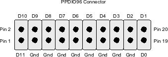
Note: The Bank connectors are called "PPDIO96 Connectors" because these pinouts appear on the PPDIO96 96-bit digital I/O board. This is different from the PPDIO96 bus connector on the Weensy 3.6 board; A daisy-chain of PPDIO96 boards can plug into the PPDIO96 bus connector with each PPDIO96 board having eight PPDIO96 (I/O) connectors. Yeah, confusing terminology. Sorry about that...
You would think that D0 on the Bank0 connector would correspond to the MCP23S17 bit 0 (say GPA0) on IC4, D1 would correspond to GPA1, ..., D7 would correspond to GPA7, D8 would correspond to GPB0, ..., and D11 would correspond to GPB3. Then Bank 1 would continue with D0 corresponding to GPB4, D1 would correspond to GPB5, ..., D3 would correspond to GPB7 on IC4, D4 would correspond to GPA0 on IC3, ... D11 would correspond to GPA7 on IC3, and the eight dip switches would correspond to GPB0...GPB7 on IC3. However, it doesn't quite happen like this. The bits are laid out on the bank connectors to make it eaiser to lay out the traces on the circuit board (between the ICs and the bank connectors). Therefore, bits get moved around and rotated on the connector. See the Weensy board layout files if you are wondering what's going on here. In any case, there is a "readBank" whose sole purpose is to make sense of all this. The readBank function lets you specify a bank number in the range 0..2. For banks zero and one this function reads 12 bits from the MCP23S17 ICs and organizes those bits in the return result to match the nomenclature on the Bank Connectors. For bank 2, the function returns the eight bits associated with the DIP switches.
Note that the readBank function only applies to the on-board MCP23S17 GPIO expanders. The off-board MCP23S17 has the bare GPAx and GPBx pins available so you read them directly.
The testSPI.ino program (given earlier) initializes the MCP23S17 as follows:
- All pins are inputs
- Pullup resistors are activated on each pin
- Input data is not inverted (raw reads)
- No interrupts are generated by the MCP23S17
In the sketch's "loop" function, the code simply reads the data for the three banks (for the on-board ICs) and the data for the off-board MCP23S17 and displays their values in hexadecimal. The main loop function reads and displays the data (to the Arduino IDE serial output display) every 100 msecs. Because the code initializes the ICs with the pullup resistors activated, by default the loop functions will display all 1 bits (0xfff or 0xff, depending on data read; this assumes all the DIP switches are in the off/open position). By shorting one of these input pins to ground (or closing a DIP switch) you can see the value change (a bit will change to zero, producing a hexadecimal value other than 0xff or 0xfff).
To test the wiring of two the on-board MCP23S17 ICs, you should manually short each data pin on the two Bank Connectors to ground (one at a time) and verify you get a zero bit (hopefully in the correct bit position). If you're reading data at all from the off-board MCP23S17, and you can get at least one value that doesn't contain all one bits, then you've probably done a sufficient test for the given SPI bus and chip select line.
The basic program (given earlier) has a default chip select value of '1' for the off-board MCP23S17. This is set with the following definition at the beginning of the program:
#define whichBS 1
You should run the program seven different times with "whichBS" set to 0...6, moving the off-board MCP23S17 chip select jumper between the BS0 through BS6 jumpers on the PPDO and PPDIO96 bus connectors. This will verify that you've properly soldered these connections (and the circuitry controlling these connections). When testing BS0, you should also move the MOSI, MISO, and SCK signals to the PPDO connector (to test those circuits).
Testing the GPIO Connector
The Weensy 3.6 contains a small 2x5 (10-pin) header that holds five addition general-purpose I/O (GPIO) pins from the Teensy 3.6. These pins run through an Adafruit TXB0108 breakout board and operation at 5v logic levels. The GPIO connector has the following pinout:
| Pin | Function |
|---|---|
| 1 | Teensy pin 34 |
| 2 | Teensy pin 33 |
| 3 | Teensy pin 39 |
| 4 | Teensy pin 28 |
| 5 | Teensy pin 40 |
| 6 | Vcc (+5V) |
| 7 | Teensy pin 41 |
| 8 | Gnd |
| 9 | Teensy pin 42 |
| 10 | Teensy pin 55 |
Probably the best way to test these pins is to program them as digital outputs and measure the voltage levels on the pins with DVM. The following sketch allows you to turn on individual pins on the GPIO connector. Run this section and measure pin voltages with a DVM:
/*
  GPIOTest (Weensy 3.6 version)
  Verifies the proper operation of the Weensy 3.6 GPIO header Circuitry

  This example code is in the public domain.
 */

#define gpio28      28
#define gpio33      33
#define gpio34      34
#define gpio39      39
#define gpio40      40
#define gpio41      41
#define gpio42      42
#define gpio55      55

#define wd_rfsh     52
#define Reset       51
#define wd_latch    54

char            inputCh = ' ';
int             pin     = 0;


// Must send a positive pulse to the TA8030s
// to refresh the watchdog timer:

void watchdogRefresh( void )
{
    digitalWrite( wd_rfsh, 1 );
    delay( 1 );
    digitalWrite( wd_rfsh, 0 );
}

// Must send a negative-going pulse to the DS1834
// chip to cause a reset. The pulse must be at least
// 350 msec wide.

void toggleReset( void )
{
        digitalWrite( Reset, 0 );
        delay( 350 );
        digitalWrite( Reset, 1 );
}

// Turn off all the digital outputs:

void clearAll( void )
{
        digitalWrite( gpio28, 0 );
        digitalWrite( gpio33, 0 );
        digitalWrite( gpio34, 0 );
        digitalWrite( gpio39, 0 );
        digitalWrite( gpio40, 0 );
        digitalWrite( gpio41, 0 );
        digitalWrite( gpio42, 0 );
        digitalWrite( gpio55, 0 );
}


// the setup routine runs once when you press reset:

void setup()
{
    Serial.begin( 9600 );
    delay( 1000 );
    Serial.println( "GPIO Test Program" );


    // Stuff needed by the watchdog timer:

    pinMode( Reset, OUTPUT );       // Reset pin is an output.
    pinMode( wd_rfsh, OUTPUT );     // Watchdog refresh is an output.
    pinMode( wd_latch, INPUT );    // Read watchdog state here.


    // GPIO data lines -- initialize as outputs:

    pinMode( gpio28, OUTPUT );
    pinMode( gpio33, OUTPUT );
    pinMode( gpio34, OUTPUT );
    pinMode( gpio39, OUTPUT );
    pinMode( gpio40, OUTPUT );
    pinMode( gpio41, OUTPUT );
    pinMode( gpio42, OUTPUT );
    pinMode( gpio55, OUTPUT );


    watchdogRefresh();              // Guarantee that the WD is refreshed
    toggleReset();                  // Reset watchdog timer latch.
    delay( 350 );
    watchdogRefresh();              // Guarantee that the WD is refreshed

    Serial.println();
    Serial.println( "Choose item to turn on:" );
    Serial.println();
    Serial.println( "a.  gpio28 (pin  4)" );
    Serial.println( "b.  gpio33 (pin  2)" );
    Serial.println( "c.  gpio34 (pin  1)" );
    Serial.println( "d.  gpio39 (pin  3)" );
    Serial.println( "e.  gpio40 (pin  5)" );
    Serial.println( "f.  gpio41 (pin  7)" );
    Serial.println( "g.  gpio42 (pin  9)" );
    Serial.println( "h.  gpio55 (pin 10)" );
    Serial.println( "anything else turns off all pins" );

}

// the loop routine runs over and over again forever:

void loop()
{
    if( Serial.available() > 0 )
    {
        inputCh = Serial.read();
        digitalWrite( gpio28, 0 );
        digitalWrite( gpio33, 0 );
        digitalWrite( gpio34, 0 );
        digitalWrite( gpio39, 0 );
        digitalWrite( gpio40, 0 );
        digitalWrite( gpio41, 0 );
        digitalWrite( gpio42, 0 );
        digitalWrite( gpio55, 0 );
        switch( inputCh )
        {
            case 'a':
                pin = gpio28;
                break;

            case 'b':
                pin = gpio33;
                break;

            case 'c':
                pin = gpio34;
                break;

            case 'd':
                pin = gpio39;
                break;

            case 'e':
                pin = gpio40;
                break;

            case 'f':
                pin = gpio41;
                break;

            case 'g':
                pin = gpio42;
                break;

            case 'h':
                pin = gpio55;
                break;

            case 0xa:
            case 0xd:
                break;

            default:
                clearAll();
                pin = 0;
                break;
        }
    }
    watchdogRefresh();
    if( pin != 0 )
    {
        digitalWrite( pin, 1 );
    }
}
Testing the Adafruit Feather Bus Connectors
The following tables describe the I/O pinouts on the Feather bus.
| Pin | Digital I/O Pin | Feather JP3 Header Function |
|---|---|---|
| 1 | -- | Gnd |
| 2 | 1 | TX1 |
| 3 | 0 | RX1 |
| 4 | 12 | MISO0 |
| 5 | 11 | MOSI0 |
| 6 | 13 | SCK0 |
| 7 | 20 | A6 (analog input 0-3.3V) |
| 8 | 14 | A0 (analog input 0-3.3V) |
| 9 | 16 | A2 (analog input 0-3.3V) |
| 10 | 17 | A3 (analog input 0-3.3V) |
| 11 | 15 | A1 (analog input 0-3.3V) |
| 12 | -- | DAC0 |
| 13 | -- | Gnd |
| 14 | -- | ARef |
| 15 | -- | 3.3v supply (max 250mA) |
| 16 | -- | Program |
Note: JP3 Pin 1 (Gnd) is located on the lower-right hand side of the Weensy 3.6 PCB when viewed from the top.
JP4 Pin 1 is closest to the utility LED (labeled "LED") on the Weensy 3.6 PCB
| Pin | Digital I/O Pin | Feather JP4 Header Function |
|---|---|---|
| 1 | VBat | |
| 2 | -- | N/C |
| 3 | -- | Vcc (3.3v) |
| 4 | 5 | Digital I/O pin 5 (3.3v only) |
| 5 | 6 | Digital I/O pin 6 (3.3v only) |
| 6 | 9 | Digital I/O pin 9 (3.3v only) |
| 7 | 10 | Digital I/O pin 10 (3.3v only) |
| 8 | 4 | Digital I/O pin 4 (3.3v only) |
| 9 | 3 | Digital I/O pin 3 (3.3v only) |
| 10 | 8 | Digital I/O pin 8 (3.3v only) |
| 11 | 19 | SCL0 (3.3v, with 10K pullup to +3.3v) |
| 12 | 18 | SDA0 (3.3v, with 10K pullup to +3.3v) |
Testing the SPI and I2C busses on the Adafruit Feather bus is probably best accomplished by using some Adafruit Featherwings based on these busses. For example, you can test the I2C bus with the Adafruit 0.56" 4-digit 7-Segment Display and you can test the SPI bus with the Featherwing OLED module. You may need to make some minor modifications to the library code Adafruit provides (to use the Teensy I2C and SPI libraries), but usually this is an easy task.
Note that with the exception of DAC0, all of the I/O pins (pins other than voltages, ground, references, and the PROGRAM pin) have a digital I/O equivalent. Therefore, the easiest test to see if all these pins are properly connected to the Teensy 3.6 module is to program them all as digital inputs and read the values from these pins (tying them, individually, to +3.3V or Gnd). The following Teensy sketch does this and displays each of the digital input values:
  FeatherTest (Weensy 3.6 version)
  Verifies the proper operation of the Weensy 3.6 Feather header Circuitry

  This example code is in the public domain.
 */

#define pin0         0
#define pin1         1
#define pin3         3
#define pin4         4
#define pin5         5
#define pin6         6
#define pin8         8
#define pin9         9
#define pin10       10
#define pin11       11
#define pin12       12
#define pin13       13      // Also affects LED on Teensy 3.6
#define pin14       14
#define pin15       15
#define pin16       16
#define pin17       17
#define pin18       18
#define pin19       19
#define pin20       20

#define wd_rfsh     52
#define Reset       51
#define wd_latch    54


// Must send a positive pulse to the TA8030s
// to refresh the watchdog timer:

void watchdogRefresh( void )
{
    digitalWrite( wd_rfsh, 1 );
    delay( 1 );
    digitalWrite( wd_rfsh, 0 );
}

// Must send a negative-going pulse to the DS1834
// chip to cause a reset. The pulse must be at least
// 350 msec wide.

void toggleReset( void )
{
        digitalWrite( Reset, 0 );
        delay( 350 );
        digitalWrite( Reset, 1 );
}

// Turn off all the digital outputs:

void clearAll( void )
{
        digitalWrite( pin0, 0 );
        digitalWrite( pin1, 0 );
        digitalWrite( pin3, 0 );
        digitalWrite( pin4, 0 );
        digitalWrite( pin5, 0 );
        digitalWrite( pin6, 0 );
        digitalWrite( pin8, 0 );
        digitalWrite( pin9, 0 );
        digitalWrite( pin10, 0 );
        digitalWrite( pin11, 0 );
        digitalWrite( pin12, 0 );
        digitalWrite( pin13, 0 );
        digitalWrite( pin14, 0 );
        digitalWrite( pin15, 0 );
        digitalWrite( pin16, 0 );
        digitalWrite( pin17, 0 );
        digitalWrite( pin18, 0 );
        digitalWrite( pin19, 0 );
        digitalWrite( pin20, 0 );
}


// the setup routine runs once when you press reset:

void setup()
{
    Serial.begin( 9600 );
    delay( 1000 );
    Serial.println( "Feather Test Program" );


    // Feather bus I/O pins:

    pinMode( pin1,  INPUT );
    pinMode( pin3,  INPUT );
    pinMode( pin4,  INPUT );
    pinMode( pin5,  INPUT );
    pinMode( pin6,  INPUT );
    pinMode( pin8,  INPUT );
    pinMode( pin9,  INPUT );
    pinMode( pin10, INPUT );
    pinMode( pin11, INPUT );
    pinMode( pin12, INPUT );
    pinMode( pin13, INPUT );
    pinMode( pin14, INPUT );
    pinMode( pin15, INPUT );
    pinMode( pin16, INPUT );
    pinMode( pin17, INPUT );
    pinMode( pin18, INPUT );
    pinMode( pin19, INPUT );
    pinMode( pin20, INPUT );

    // Stuff needed by the watchdog timer:

    pinMode( Reset, OUTPUT );       // Reset pin is an output.
    pinMode( wd_rfsh, OUTPUT );     // Watchdog refresh is an output.
    pinMode( wd_latch, INPUT );    // Read watchdog state here.


    watchdogRefresh();              // Guarantee that the WD is refreshed
    toggleReset();                  // Reset watchdog timer latch.
    delay( 350 );
    watchdogRefresh();              // Guarantee that the WD is refreshed

}

// the loop routine runs over and over again forever:

void loop()
{
    char outStr[256];

    sprintf
    (
        outStr,
        "JP3[P2:%d, P3:%d, P4:%d P5:%d P6:%d P7:%d P8:%d P9:%d P10:%d P11:%d]    ",
        digitalRead( pin1 ),
        digitalRead( pin0 ),
        digitalRead( pin12 ),
        digitalRead( pin11 ),
        digitalRead( pin13 ),
        digitalRead( pin20 ),
        digitalRead( pin14 ),
        digitalRead( pin16 ),
        digitalRead( pin17 ),
        digitalRead( pin15 )
    );
    Serial.print( outStr );

    sprintf
    (
        outStr,
        "JP4[P4:%d, P5:%d, P6:%d P7:%d P8:%d P9:%d P10:%d P11:%d P12:%d]",
        digitalRead( pin5 ),
        digitalRead( pin6 ),
        digitalRead( pin9 ),
        digitalRead( pin10 ),
        digitalRead( pin4 ),
        digitalRead( pin3 ),
        digitalRead( pin8 ),
        digitalRead( pin19 ),
        digitalRead( pin18 )
    );
    Serial.println( outStr );


    watchdogRefresh();
    delay( 250 );
}
Note that Teensy Pin 13 (JP3 Pin 6) is tied to the Teensy 3.6's LED (and then to ground). Therefore, this pin will always read zero if nothing is connected to JP3 pin 6. If you tie this to +3.3V (either JP3 Pin 15 or the Weensy 3.3v test point) then you should read a '1' on the input (and the LED should illuminate). All of the other pins are floating; floating pins usually read as a '1' (though this isn't guaranteed). Tying any of these pins to Gnd (JP3 Pin 1) should produce a zero on output, tying these pins to +3.3V (either JP3 Pin 15 or the Weensy 3.3v test point) will produce a '1' on the program's output display.
You can also hook up a potentiometer (outside leads between +3.3v and ground with the center lead to an analog input) and measure the correct operation of the analog inputs. However, if the pins work properly as digital inputs, it's hard to imagine they won't also work as analog inputs (this is a Teensy function, not so much a Weensy function).
The following is a modification of the triangle wave program given earlier (when testing the I2C bus) that sends a triangle wave to the Teensy 3.6's DAC0 port (which comes out on pin 12 of JP3 on the Feather headers). This produces a higher-frequency square wave than the earlier example, because the Teensy's DAC is much faster than the I2C DAC found on the Adafruit MPC4725 breakout board. You can verify the production of the triangle wave with an oscilloscope to verify that this pin on the Feather bus is working.
/**************************************************************************/
/*!
    @file     DACTest.ino
    @author   Adafruit Industries + Randy Hyde
    @license  BSD (see license.txt)

    This example will generate a triangle wave with the MCP4725 DAC.

    This is an example sketch for the Adafruit MCP4725 breakout board
    ----> http://www.adafruit.com/products/935

    Adafruit invests time and resources providing this open source code,
    please support Adafruit and open-source hardware by purchasing
    products from Adafruit!
*/
/**************************************************************************/


#define LEDPin      2
#define Reset       51
#define wd_rfsh     52


// Must send a positive pulse to the TA8030s
// to refresh the watchdog timer:

void watchdogRefresh( void )
{
    digitalWrite( wd_rfsh, 1 );
    digitalWrite( wd_rfsh, 0 );
}

// Must send a negative-going pulse to the DS1834
// chip to cause a reset. The pulse must be at least
// 350 msec wide.

void toggleReset( void )
{
        digitalWrite( Reset, 0 );
        delay( 350 );
        digitalWrite( Reset, 1 );
}

// Test code to generate a triangle wave:


void setup(void)
{
    Serial.begin(9600);
    delay( 1000 );
    Serial.println("DAC0 Test program for Feather Bus");

    analogWriteResolution(12);
    pinMode( wd_rfsh, OUTPUT );
    pinMode( LEDPin, OUTPUT );
    pinMode( Reset, OUTPUT );

    watchdogRefresh();
    toggleReset();
    delay( 350 );
    watchdogRefresh();

    Serial.println("Generating a triangle wave");
}

void loop(void)
{
    uint32_t counter;

    // Run through the full 12-bit scale for a triangle wave

    digitalWrite( LEDPin, 0 );
    for (counter = 0; counter < 4095; counter++)
    {
        analogWrite(A21, counter);
    }
    watchdogRefresh();

    digitalWrite( LEDPin, 1 );
    for (counter = 4095; counter > 0; counter--)
    {
        analogWrite(A21, counter);
    }
    watchdogRefresh();
}
Testing the Weensy DAC Header
Testing the DAC header on the Weensy is relatively easy. Use the triangle wave test program from the previous section and measure the output on the DAC header (pins 0 + G) and verify with an oscilloscope that you're getting a triangle wave. Then modify the program and replace the two "analogWrite(A21, counter);" statements with "analogWrite(A22, counter);" Now you should see a triangle wave on pins 1 + G on the DAC header.
Testing the Weensy AIN Header
The Weensy 3.6 AIN brings out pins A10 and A11 (that have no other secondary functions on the Teensy). By hooking up a potentiometer between +3.3v and the pot's center lead to either the A0- (A11) or A0+ (A10) leads on the Weensy AIN header, you can test the analog input pins. The following code accomplishes this:
// ADCTest-
//
//  Tests the analog input pins on the Weensy 3.6


#define LEDPin      2
#define Reset       51
#define wd_rfsh     52


// Must send a positive pulse to the TA8030s
// to refresh the watchdog timer:

void watchdogRefresh( void )
{
    digitalWrite( wd_rfsh, 1 );
    digitalWrite( wd_rfsh, 0 );
}

// Must send a negative-going pulse to the DS1834
// chip to cause a reset. The pulse must be at least
// 350 msec wide.

void toggleReset( void )
{
        digitalWrite( Reset, 0 );
        delay( 350 );
        digitalWrite( Reset, 1 );
}

// Test code to generate a triangle wave:


void setup(void)
{
    Serial.begin(9600);
    delay( 1000 );
    Serial.println("AIN Test program for Weensy 3.6");

    pinMode( wd_rfsh, OUTPUT );
    pinMode( LEDPin, OUTPUT );
    pinMode( Reset, OUTPUT );

    watchdogRefresh();
    toggleReset();
    delay( 350 );
    watchdogRefresh();

}

void loop(void)
{
    uint32_t counter;
    uint16_t A0p    = analogRead( A10 );
    uint16_t A0m    = analogRead( A11 );
    Serial.print( "A0+: " );
    Serial.print( A0p, 16 );
    Serial.print( "  A0-: " );
    Serial.println( A0m, 16 );
    delay( 250 );
    watchdogRefresh();
}
Connecting DAQ System Boards to the Weensy 3.6 Board
The Weensy 3.6 board provides 10 separate headers/connectors you can use to connect PPOPTO-12, PPRLYIO-12, PPDIO96, PPRelay-12, PPSSR-16, and PPAIO-16/4 boards. There are also two four-pin I2C connectors you can use to connect additional I2C devices (beyond the PPAIO-16/4 boards) and a 3-pin header connecting to the watchdog relay.
Connections to these devices is that same as for Plantation Productions Incorporated's DAQ_IF boards. See the following web pages for more details:
- DAQ_IF board
- PPAC4 board
- PPAC420 board
- PPAIO-16/4 board
- PPBreakin board
- PPBreakout board
- PPDIO96 board
- PPOpto-12 board
- PPRelay-12 board
- PPRlyio-12 board
- PPSSR-16 board
Note: all of the DAQ system boards (above) are open-source/open-hardware covered under the Creative Commons Attribution International 4.0 license.
Connecting PPOpto-12 and PPRlyio-12 Boards to the Weensy
Because the Weensy 3.6 board supports two PPDIO96 Bank connectors, you can connect PPOpto-12 and PPRlyio-12 boards directly to these connectors. The PPOpto-12 board provides 12 channels of optical isolation for digital inputs (see the PPOpto-12 web page for more details). The PPOpto-12 accepts dry contact (switch) inputs or logic-level inputs (between +5V and +15V). You would connect a PPOpto-12 board (or two) to the Weensy 3.6 as follows:
Note that PPOpto-12 boards are input-only devices. They take digital inputs from the outside world (external to the Weensy hardware) and make that input data available in an isolated 5v-logic (TTL) form for the Weensy 3.6.
The Plantation Productions' PPRlyio-12 board (see the web page here) is also compatible with the PPDIO96 Bank connectors found on the Weensy 3.6. Therefore, you can connect PPRlyio-12 boards to the Weensy Bank 0 and Bank 1 connectors. Unlike the PPOpto-12, the PPRlyio-12 board can be either an input or an output device (note that all 12 I/O signals must be input or output, you cannot have a mixture of both without some serious hacking). As an input device, the PPRlyio-12 accepts a TTL-compatible (5v) logic signal as input, buffers (and possibly inverts) this signal, and makes it availble to the Weensy 3.6 board. Note that the PPRlyio-12 board does not isolate the input signal from the Weensy; from the electrical perspective of the Weensy the PPRlyio-12 simply buffers (amplifies) the signal. In addition to making the input signal available to the Weensy, the PPRlyio-12 board also activates a mechanical relay if the signal is active (can be active-high or active-low, jumper programmable). You can use this relay to control some other item in your system. Note that the relay contact (NO/COM/NC) are isolated from the rest of the system. Here's how you can hook up the PPRlyio-12 board to the Weensy:
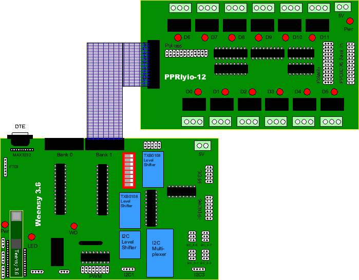
Note that the PPRlyio-12 board buffers the digital inputs sent to the Weensy (as wired above) using ULN2308 darlington transistor arrays. These are open-collector devices and normally you must supply pull-up resistors to obtain TTL-level signals. Although the PPRlyio-12 board has (jumper-selectable) pullup resistor present, you don't really need to use these as the MCP23S17 provides programmable pullup resistors on all input pins. See the PPRlyio-12 and MCP23S17 data sheets/web pages for more details.
The PPRlyio-12 board has two PPDIO96-Bank-Compatible headers on it: an input header and an output header. When using the PPRlyio-12 board as an input device to the Weensy 3.6 board, you connect the output header on the PPRlyio-12 board to one of the Bank connectors on the Weensy 3.6. You can then connect your digital inputs to the PPDIO96 Bank In connector on the PPRlyio-12 board. The PPRlyio-12 board "sits in the middle" of your digital signal path and actuates the relays as well as providing those input signals to the Weensy 3.6.
If you need isolated inputs as well as relay control on the inputs, you can daisy chain a PPOpto-12 and PPRlyio-12 board together to provide this functionality. Connect the PPOpto-12's bank connector to the PPRlyio-12 Bank In connector and then connect the PPRlyio-12 Bank Out connector to one of the PPDIO96-Compatible Bank connectors on the Weensy 3.6:
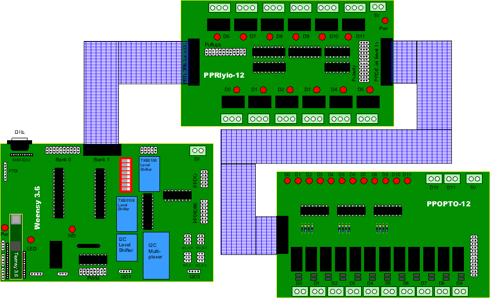
The MCP23S17 GPIO expander ICs also allow you to program the pins on the Bank connectors as outputs (in addition to inputs). It is possible to use the PPRlyio-12 as an output device by connecting on the bank connectors on the Weensy 3.6 to the PPDIO96 Bank In connector on the PPRlyio-12:
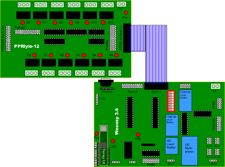
In this scenario, writing to an output bit on the MCP23S17 GPIO ICs turns on or off one of the relays on the PPRlyio-12 board (it also passes a buffered version of this signal on to the PPDIO96 Bank Out connector on the PPRlyio-12 board). Note that the relay contact outputs are naturally isolated from the rest of the system; the buffered outputs (on the PPRlyio-12's PPDIO96 Bank Out connector) are buffered but not isolated.
Connecting PPDIO96 Boards to the Weensy 3.6
If the addition 24/32 bits of digital I/O provided by the two on-board MCP23S17 GPIO expander ICs is insufficient for your needs, you can always add additional digital I/O pins via the PPDIO96 board. Each PPDIO96 board adds 96 bits of digital I/O to the system. The PPDIO96-Bus compatible connector suppports up to six PPDIO96 boards for a grand total of 576 additional I/O bits. Seriously, though, one (or two) PPDIO96 boards is probably enough for most systems, but have the ability to add up to six PPDIO96 boards means it's highly unlikely you'll run out of digital I/O lines on a Weensy system.
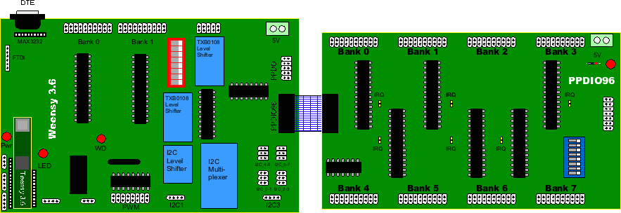
Each PPDIO96 board adds eight PPDIO96 Bank connectors to your system. You can access the pins on these connectors directly or add PPOpto-12 and PPRlyio-12 boards to these connectors just as you would to the two Bank connectors on the Weensy board.
You can "daisy-chain" multiple PPDIO96 boards off the Weensy's PPDIO96 bus connector. The first board connects to the PPDIO96 bus connector on the Weensy, the second board attaches to the PPDIO96 bus connector on the right-hand side of the first board, the third connects to the PPDIO96 bus connector on the second board, etc.
The "board select" signal increases by one for each PPDIO96 you add to the system. That is, the MCP23S17 ICs on the first board respond to the BS1 board select signal, the second board responds to BS2, etc. In the example MCP23S17 code given earlier, you used BS7 for the on-board MCP23S17 and BS1 for the remaining tasks. You use BS1...BS6 to select the six possible PPDIO96 boards daisy-chained to the Weensy 3.6.
For more information on programming the PPDIO96 boards, see the PPDIO96 web page documentation and the MCP23S17 data sheet.
Connecting PPRelay-12 and PPSSR-16 Boards to the Weensy 3.6
The Plantation Productions' DAQ (data acquisition) system provides two separate relay output boards that attach to the PPDO bus connector on the Weensy 3.6: the PPRelay-12 and the PPSSR-16 boards. The PPRelay-12 board provides 12 mechanical relays and four digital output pins. The PPSSR-16 provides 16 Solid-State Relays (SSRs).
The PPRelay-12 board provides 12 mechanical SPDT relays (NO/COM/NC contacts) capable of handling a couple amps at 30VDC (they will also handle 220VAC, but I do not recommend bringing AC directly to the relay boards as they are not finger safe – instead send a logic signal to a relay somewhere else where you can ensure that high-voltages are not present in a form that someone could shock themselves.
Note: the relays on the PPRelay-12 board are rated at 5 amps. Good engineering practice suggests that you always derate the capacity by 50%, so assume 2.5A. Also, the traces on the board will start to get warm (hot) if you run a fair amount of current through them, so I'd limit myself to 1-2A (and 2A on an intermittent basis).
Like the PPDIO96 boards, you can daisy-chain a sequence of PPRelay-12 and PPSSR-16 boards off the PPDO bus connector. Each board looks like a 16-bit serial-in, parallel-out shift register. Daisy-chaining them extends the size of the shift register. In theory, you could add as many shift registers as you like to the system; in practice, you should probably limit yourself to fewer than 10 boards to avoid TTL-fanout problems.
Here is a typical connection involving one PPRelay-12 board:
You can daisy-chain additional PPRelay-12 or PPSSR-16 boards to he PPDO Out bus connector on the PPRelay-12 board.
The PPRelay-12 board offers a couple advantages for digital output over using a PPRlyio-12 board connected to a PPDIO96-Compatible Bank connector:
- PPRelay-12 boards provide fail-safe operation. On power up, after a reset operation, or whenever the watchdog timer on the Weensy expires, the PPRelay-12 board turns all relays off. This is not guaranteed on PPRlyio-12 board (indeed, it is often the case that the PPRlyio-12 relays, used at outputs from a PPDIO96 Bank connector, will be turned on under these conditions, though even that is not guaranteed as the inputs to the PPRlyio-12 board will be floating at that point).
- PPRelay-12 boards are simpler; therefore they are less costly and easier to build.
- PPRelay-12 boards actually provide 16 outputs; four output pins are available on an auxiliary connector. The PPSSR-16 boards, obviously, also provide 16 outputs. The PPRlyio-12 board only provides 12 outputs.
- Mapping the output bits to the relays is much easier with the PPRelay-12 and PPSSR-16 bits (it's just a long serial shift register). The PPDIO96 boards have some crazy bit mapping going on (in order to simplify the PCB layout for the circuit board). Therefore, it's easier to program the PPRelay-12 and PPSSR-16 boards than it is to program the PPDIO96/PPRlyio-12 (or Weensy/PPRlyio-12) boards.
Analog I/O Expansion Using the PPAIO-16/4, PPAC4, and PPAC420 Boards
The Plantation Productions' DAQ system include a set of boards to provide analog I/O as well as analog signal conditioning.
The PPAIO-16/4 provides 16 single-ended (8 differential) 16-bit A/D converters and four 12-bit single-ended D/A converters. This boards is based on the Adafruit and Sparkfun ADS1115 (ADC) and MCP4725A (DAC) breakout boards. These are I2C devices so the PPAIO-16/4 boards connect to the Weensy 3.6 board using the four sets of 2x3 (6-pin) headers (I2C3-0/1, I2C3-2/3, I2C3-4/5, and I2C3-6/7). You can daisy-chain two boards off each of these 6-pin connectors (total of eight boards), yielding a grand total of 128 possible analog inputs (single-ended, 64 differential inputs) and 32 digital outputs.
You can connect a PPAIO-16/4 to any of the 6-pin I2C3 connectors; convention, however, is to connect the first board to I2C3-0/1, the second board to I2C3-2/3, the third board to I2C3-4/5, and the fourth board to I2C3-6/7. The next four boards (boards 5-8) daisy-chain to the first four boards (in order). There are some specific limitations on the assembly of the boards if you add more than four boards to the system (or choose to use daisy-chaining). Please see the PPAIO-16/4 documentation (web page) for more details.
The PPAIO-16/4 provides on-board analog conditioning for the DAC circuits. Specifically, you have the ability to produce output voltages in the range ±10V or ±5V rather than the standard (MCP4725A) 0...5V range. You can adjust the output voltage range using jumpers and pots directly on the PPAIO-16/4 board. See the documentation for more details.
The ADS1115 I2C ADC (provided on Adafruit breakout boards) is a 16-bit, modest speed (max 860 conversions/second), device than handles 0...4.096V inputs at full range or 0...5V with slightly less than a 16 bit input range. In industrial settings, 0...10V or ±10V input ranges are more common. Furthermore, in industrial settings you really want the input signal isolated from the rest of the circuitry. To overcome these issues, Plantation Productions has designed the PPAC4 four-channel analog conditioning module. The PPAC4 provides isolation amplifiers (along with isolated power supplies) and various op-amp circuitry to all the input of ±5V and ±10V signals, producing differential outputs (you can adjust the ranges on the outputs, but typically they would be set to 0...4.096V to maximize the conversion range of the ADS1115).
Because the PPAC4 produces a differential signal, you can send the output (from the PPAC4) over a greater distance than would be possible with single-ended outputs. The drawback to using differential signals is that it takes two analog inputs to handle a single differential signal, cutting the number of analog inputs by half. The PPAC4 has four two-pin screw terminals for inputs and four corresponding two-pin screw terminals for outputs. You would normally connect the "plus" output to an even-numbered analog input (non-ground input) and the "minus" output to an odd-numbered analog input (non-ground pin) on the PPAIO-16/4. See the PPAC4 documentation for more details.
High-resolution image shot with a Canon EOS 5D MII
In many industrial settings an analog input is provided in a current-loop form rather than a voltage. The PPAC420 board provides eight channels of 4-20mA to 5V conversion. You would typically connect a current loop input to one of the inputs on the PPAC420 and then connect the corresponding output to one of the inputs on a PPAC4 board (whose output would then connect to a PPAIO-16/4 board). Note that the PPAC420 produces 0...5V for current in the range 4...20mA. It produces an output voltage in the range -1.25..0V for current in the range 0..4 mA. Because the ADS1115 ADC really doesn't like negative voltages, you must run the output of the PPAC420 through the PPAC4 to handle this issue (not to mention add isolation and produce a full-range 16-bit output from the ADC). For more details on the PPAC420, check out the documentation.
High-resolution image shot with a Canon EOS 5D MII
Programming the Weensy 3.6 Board
This section is a recap of several of the programming examples appearing earlier in this document.
I2C Busses and I2C Multiplexor
The Adafruit TCA9548A Breakout Board (BoB) responds to I2C address 0x70 on the Weensy I2C bus #3 (SDA3/SCL3). Writing a byte to this I2C address with a single bit set will activate the corresponding I2C bus on the Weensy 3.6 board (there are 8 I2C busses -- I2C_0 through I2C_7). Writing a one in bit position zero makes bus I2C_0 active; writing a one to bit position 1 makes bus I2C_1 active; etc. Once a bus is active, it remains active until you write a different value to the TCA9548A BoB. Writing a zero to the TCA9548A BoB disables all eight I2C busses on the multiplexor.
Reset
Programming a low pulse on the reset output pin will send a reset signal to all the devices in the DAQ peripheral system. You must program this pin low for at least 250 msec. The reset signal has the following effects throughout the system:
- Resets the watchdog timer. Note that this is the only way to reset the watchdog timer latch. Therefore, you should always send a reset pulse when the system first powers up.
- Resets the on-board MCP23S17 GPIO expander chips. Note that this reprograms all the digital I/O pins as inputs and disables all pull-up resistors. If you've programming any pins as outputs or if you've enabled any programmable pull-up resistors on the MCP23S18, you will need to reinitialize the I/O expander after pulsing the reset line.
- Resets the MCP23S17 GPIO expander chips on the PPDIO96 boards attached to the Weensy 3.6. Note that this reprograms all the digital I/O pins as inputs and disables all pull-up resistors. If you've programming any pins as outputs or if you've enabled any programmable pull-up resistors on the MCP23S18, you will need to reinitialize the I/O expander after pulsing the reset line.
- Puts all the output relays on the PPRelay-12 and PPSSR-16 boards in fail-safe mode (open relay contacts).
The reset line is digital I/O pin #51 on the Teensy 3.6:
#define Reset	 	51

// In setup function:

    pinMode( Reset, OUTPUT );

// Elsewhere:

void toggleReset( void )
{
		digitalWrite( Reset, 0 );
		delay( 250 );
		digitalWrite( Reset, 1 );
}
Watchdog Refresh
Programming a rising edge on the WD_RFSH output pin will refresh the Weensy 3.6's on-board watchdog timer hardware. You must program at least one pulse every five seconds (or faster) to prevent the watchdog timer from "timing out" and activating the watchdog timer relay.
The reset line is digital I/O pin #51 on the Teensy 3.6:
#define wd_rfsh     52

// In setup function:

    pinMode( wd_rfsh, OUTPUT );


// Elsewhere:

// Must send a positive pulse to the TA8030s
// to refresh the watchdog timer:

void watchdogRefresh( void )
{
    digitalWrite( wd_rfsh, 1 );
    delay( 1 ); // A full millisecond isn't really needed, but it doesn't hurt
    digitalWrite( wd_rfsh, 0 );
}
Watchdog Latch Input
The watchdog latch input pin gives you an indication of the current watchdog timeout state. If you read a '1' on this input pin, then the watchdog timer has latched the "timeout" state. If you read a '0' on this pin, the watchdog timer has not timed out.
Note that once the watchdog timer times out, the watchdog timeout state is latched until the software explicitly resets it. Note that refreshing the watchdog timer once it has timed out will not reset the watchdog timer. You must pulse the reset signal (as noted above) to reset the watchdog timer.
#define wd_latch    54

// In setup function:

    pinMode( wd_rfsh, INPUT );


// Elsewhere:


latchStatus = digitalRead( wd_latch );
IRQ Input
The IRQ input signal is connected to the INTA lines on the MCP23S17 I/O expanders (onboard as well as those found on the PPDIO96 board). Note that the IRQ jumper with a given MCP23S17 must be installed for this signal to work. If you want to use this feature on the Weensy 3.6 you'd normally program pin 53 on the Teensy 3.6 as an interrupt and write an interrupt service routine to process the interrupt. You could also poll this input pin if writing an interrupt service routine isn't appropriate.
J2_38 Pin
The J2_38 pin is an application-defined I/O pin that is present on the PPDIO96 and PPDO busses. It is connected to Teensy 3.6 pin #47. The Weensy system does not use this pin; it's left for your own use. You may program it as an input or an output depending on your needs. Commonly, programms use this signal to send a pulse to an oscilloscope or logic analyzer for timing purpose.
BTW: this pin gets its name from the Netburner MOD54415 board connecting to a Plantation Productions' DAQ_IF board (on which the Weensy 3.6 is based). It's pin 38 on header J2.
PWM Pins
The Weensy 3.6 brings out eight (otherwise unused) output pins that provide PWM (pulse width modulation). The Weensy 3.6 PCB connects these eight pins directly to a ULN2308 darlington array that provides up to 500ma sink capability per pin. Although the Teensy 3.6 normally allows you to program these pins as either inputs or outputs, because of the wiring on the Weensy 3.6 you will always program these pins as outputs.
The Teensy 3.6 pins connected to the ULN2308 are:
- Pin 7
- Pin 21
- Pin 22
- Pin 23
- Pin 29
- Pin 30
- Pin 35
- Pin 36
    #define pwm7        7
    #define pwm21       21
    #define pwm22       22
    #define pwm23       23
    #define pwm29       29
    #define pwm30       30
    #define pwm35       35
    #define pwm36       36

    // In the setup function:


    // PWM output lines -- always outputs:

    pinMode( pwm7, OUTPUT );
    pinMode( pwm21, OUTPUT );
    pinMode( pwm22, OUTPUT );
    pinMode( pwm23, OUTPUT );
    pinMode( pwm29, OUTPUT );
    pinMode( pwm30, OUTPUT );
    pinMode( pwm35, OUTPUT );
    pinMode( pwm36, OUTPUT );
You can use the Arduino/Teensy digitalWrite function to control these outputs. Note that ULN2308 ICs create a closed circuit to ground when an input pin is programmed with a '1' and create an open circuit (respect to ground) when the input pin is '0'. The ULN2308 ICs do not source current, they only sink current (that is, they switch theirpins to ground, not to Vcc).
The ULN2308 are capable of controlling small relays, motors, and other inductive loads but you must insert flyback diodes into the circuit to prevent damage to the Weensy 3.6 board (look at the PPRelay-12 design if you don't understand where the flyback diode goes). Do not assume the diodes built into the ULN2308 package will suffice. The ULN2308 will easily control LEDs and other non-inductive loads that work by applying Vcc to one pin and having the ULN2308 pull the other pin to ground.
Note that the header on the Weensy 3.6 board is a 16-pin header. Eight of the pins are connected to +5V and the other eight pins are connected to the ULN2308 (which effectively become the ground pin when the output is actuated). Although each ULN2308 channel could draw as much as 500ma, it would not be wise to pull 500 ma on all eight channels. The ULN2308 could handle this (and you can solder two of them together in parallel if you needed even more current capability per channel). However, drawing 4 amps though the Weensy 3.6 board is definitely not a good idea. If you need to draw significantly more power than 100ma per channel, you should consider using relays (solid state or mechanical) and move the current/power off the Weensy 3.6 board.
GPIO Pins
The Weensy 3.6 brings out eight (otherwise unused) general-purpose pins to a header on the board. Of course, there are two MCP23S17 GPIO expander ICs on the Weensy 3.6 that provide 24 general-purpose I/O pins and eight inputs (connected to a DIP switch). However, programming the pins directly on the Teensy 3.6 is much easier, faster, and more efficient than programming I/O pins on the MCP23S17 ICs. Therefore, for high-performance applications the eight GPIO pins can be quite useful.
The GPIO pins run through an Adafruit level-shifter breakout board and are all TTL/5V compatible.
Note: the Feather bus also has between 7 and 16 GPIO pins available if you are not otherwise using the Feather bus. Note, however, that these pins are 3.3V only.
The Teensy 3.6 pins connected to the GPIO pins are:
- Pin 7
- Pin 21
- Pin 22
- Pin 23
- Pin 29
- Pin 30
- Pin 35
- Pin 36
    #define GPIO28      28
    #define GPIO33      33
    #define GPIO34      34
    #define GPIO39      39
    #define GPIO40      40
    #define GPIO41      41
    #define GPIO42      42
    #define GPIO55      55

    // In the setup function:


    // GPIO lines - can be input or output
    // (output here for demonstrative purposes).

    pinMode( GPIO28, OUTPUT );
    pinMode( GPIO33, OUTPUT );
    pinMode( GPIO34, OUTPUT );
    pinMode( GPIO39, OUTPUT );
    pinMode( GPIO40, OUTPUT );
    pinMode( GPIO41, OUTPUT );
    pinMode( GPIO42, OUTPUT );
    pinMode( GPIO55, OUTPUT );
You can use the Arduino/Teensy digitalRead and digitalWrite functions to control these pins. Note that the 3.3V output from the Teensy 3.6 is routed through an Adafruit level shifter breakout board. These breakout boards provide voltage levels only and are incapable of sourcing or sinking much current. If your connections consume much current, you will need to buffer these pins.
Analog I/O Pins
The Weensy 3.6 brings out seven pins to a pair of headers specifically intended for analog I/O.
The DAC header contains three pins:
- Ground
- DAC 1 (alternate function: analog input A22)
- DAC 0 (alternate function: analog input A21)
The ADC header contains four pins:
- AGND (analog ground)
- ARef (analog reference)
- A10 (also differential '+' input)
- A11 (also differential '-' input)
Although the Teensy 3.6 has multiple "analog input" pins (see the Teensy 3.6 documentation), the truth is that the device really has only two ADC circuits built into the chip. Internally, an analog multiplexer switches between the various pins. On the Weensy 3.6 board, two of the analog inputs are brought out to the header so you can make use of the two ADCs directly (perhaps as a differential pair). Of course, you can still use the analog multiplexer with the Feather and GPIO pins (programmed as analog inputs), but in a Weensy 3.6 system if you really want more analog inputs (and outputs) a better way to do this is via the PPAIO-16/4 board. The Weensy 3.6 supports up to 128 single-ended (64 differential) analog inputs and up to 32 digital outputs by attaching PPAIO-16/4 boards to the Weensy 3.6. The advantage of the on-chip ADCs is that they are faster than I2C-based ADCs on the PPAIO-16/4 boards.
LED Control
The Teensy 3.6, like most Arduino-compatible CPU boards, connects an on-board LED to digital output pin 13. Unfortunately, pin 13 is also used for SCK0 (the SPI clock on the Feather bus). If you're not using the Feather bus (or the SPI connector on it) then you can program the Teensy's LED by writing a one or zero to this pin. However, if you are using the Feather's SPI bus, this function is not available. For this reason, the Weensy 3.6 includes an LED (and appropriate transistor driver) connected to digital output pin 2 on the Teensy 3.6. Writing a 1 to this pin turns the LED on, writing a zero turns the LED off.
Adafruit Feather-Compatible Bus
The Weensy 3.6 includes a pair of headers that implement Adafruit's Feather bus (as implemented on their Teensy 3.2 Feather Adapter). The pinouts for these two (female) headers is the following:
| Feather Pin # | Name | JP3 Description |
|---|---|---|
| 1 | VBat | A 3V coin cell battery between this pin and ground provides power for the Teensy 3.6's RTC. |
| 2 | N/C | Not available on the Teensy Feather. |
| 3 | Vcc | 5V source from Weensy 3.6 power supply |
| 4 | GPIO pin 5 | Digital I/O line corresponding to pin 5 on the Teensy |
| 5 | GPIO pin 6 | Digital I/O line corresponding to pin 6 on the Teensy |
| 6 | GPIO Pin 9 | Digital I/O line corresponding to pin 9 on the Teensy |
| 7 | GPIO Pin 10 | Digital I/O line corresponding to pin 10 on the Teensy |
| 8 | GPIO Pin 4 | Digital I/O line corresponding to pin 4 on the Teensy |
| 9 | GPIO Pin 3 | Digital I/O line corresponding to pin 3 on the Teensy |
| 10 | GPIO Pin 8 | Digital I/O line corresponding to pin 8 on the Teensy |
| 11 | SCL0 | I2C clock line |
| 12 | SDA0 | I2C data line |
Note: Pin 1 on the small Feather header is the pin closest to the middle of the Teensy 3.6 module.
| Feather Pin # | Name | JP4 Description |
|---|---|---|
| 1 | Gnd | Signal ground |
| 2 | Tx1 | Serial 1 transmit signal (3.3V, not RS-232 compatible) |
| 3 | Rx1 | Serial 1 receive signal (3.3V, not RS-232 compatible) |
| 4 | MISO0 | Teensy 3.6 SPI bus #0, MISO signal |
| 5 | MOSI0 | Teensy 3.6 SPI bus #0, MOSI signal |
| 6 | SCK0 | Teensy 3.6 SPI bus #0, clock signal |
| 7 | A6 | Teensy 3.5 ADC #6 |
| 8 | A0 | Teensy 3.5 ADC #0 |
| 9 | A3 | Teensy 3.5 ADC #3 |
| 10 | A2 | Teensy 3.5 ADC #2 |
| 11 | A1 | Teensy 3.5 ADC #1 |
| 12 | DAC0 | Teensy 3.6 DAC #0 output (note: pin can be reprogrammed) |
| 13 | Gnd | Signal ground |
| 14 | ARef | Reference voltage for Teensy 3.6 ADC (see Teensy documentation for limits) |
| 15 | 3.3V supply | 3.3V, maximum 250ma, from the Teensy 3.6 module (voltage regulator on Teensy) |
| 16 | Program | Teensy 3.6 PROGRAM signal |
Note: Pin 1 on the large Feather header is the pin closest to the middle of the Weensy 3.6 PCB (closest to the SD card socket on the Teensy 3.6 module).
Note that the Feather pins are connected directly to the Teensy 3.6 with no level shifting or buffering (just as with the Teensy 3.2 module). All signals are 3.3V only! As most (commercially available) Featherwings are designed for 3.3V systems, this shouldn't be an issue unless you develop your own Featherwings or just plug wires directly into the Feather headers.
Of course, most pins on the Teensy 3.6 are function reprogrammable, so it's quite possible for you to change an analog input to a digital I/O pin or a digital I/O pin to an analog input. See the Teensy 3.6 documentation for more details.
SPI Bus Programming
The Weensy 3.6 brings out two Teensy 3.6 SPI busses. SPI bus #0 is a 3.3V variant that comes out on the Feather bus (pins 4, 5, and 6 on the larger header and one of the digital I/O lines used as a chip select). SPI bus #2 comes out on the PPDIO96 and PPDO busses (as well as controlling the on-board MCP23S17 GPIO expander ICs) and is a 5V TTL-compatible bus. If you're wondering, the pins associated with SPI bus #1 on the Teensy 3.6 are used for a different function, there is no SPI bus #1 available on the Weensy 3.6.
The Weensy 3.6 provides a 74HC138 3-to-8 decoder to provide SPI bus chip select expansion. The 74HC138 has four input pins: the SPI chip select pin (which acts as a chip select to the 74HC138 IC) and three SPI address lines: pins A0, A1, and A2. To program a specific SPI device you must first program output pins A0, A1, and A2 with a three-bit binary number. Then you activate the SPI chip select line and do the SPI transmission. When the transmission is complete, you deactivate the SPI chip select line (note: activating and deactivating the SPI chip select line is often handled in library code or by hardware -- you might not need to explicitly program this pin).
The DAQ system reserves the eight possible chip select lines (BS0, BS1, ..., BS7) for the following purposes:
- BS0 (used by/shared byPPRelay-12 and PPSSR-16 boards)
- BS1: selects the first PPDIO96 board in the daisy chain.
- BS2: selects the second PPDIO96 board in the daisy chain.
- BS3: selects the third PPDIO96 board in the daisy chain.
- BS4: selects the fourth PPDIO96 board in the daisy chain.
- BS5: selects the fifth PPDIO96 board in the daisy chain.
- BS6: selects the sixth PPDIO96 board in the daisy chain.
- BS7 selects the on-board MCP23S17 I/O expanders.
#define SPICS       43
#define MOSI        44
#define MISO        45
#define SCK         46
#define CSA2        48
#define CSA1        49
#define CSA0        50

// In the setup function:

    // SPI chip select lines -- always outputs:

    pinMode( SPICS, OUTPUT );
    pinMode( CSA0, OUTPUT );
    pinMode( CSA1, OUTPUT );
    pinMode( CSA2, OUTPUT );
    digitalWrite( SPICS, 1 );   // Disable SPI chip select lines
    digitalWrite( CSA0, 0 );
    digitalWrite( CSA1, 0 );
    digitalWrite( CSA2, 0 );

    SPI2.begin();


// PPDO bus output example:

      SPI2.beginTransaction( WeensySPI );
      digitalWrite( CSA0, 0 );  // PPDO bus is board select #0
      digitalWrite( CSA1, 0 );  // so write zeros to A0, A1, and
      digitalWrite( CSA2, 0 );  // A2.
      digitalWrite( SPICS, 0 ); // Activate chip select line.

      // Only writing, incoming data is ignored:

      SPI2.transfer( 0xff);
      SPI2.transfer( 0xff );
      SPI2.transfer( 0xff);
      SPI2.transfer( 0xff );

      digitalWrite( SPICS, 1 ); // Deactivate chip select line
      SPI2.endTransaction();
PPDO Programming
As mentioned earlier, the boards daisy-chained to the PPDO connector look like a single shift register to the Weensy 3.6 board. Adding more PPRelay-12 or PPSSR-16 boards to the daisy chain (specifications allow a maximum of 10 boards -- this is limited by TTL fanout) extends the size of the shift register by 16 bits for each board you add.
To program this "shift register" you must first pull the BS0 line low (That is, set CSA0, CSA1, and CSA2 all to zero and then set the SPICS line low). Next, you transmit the specified number of bytes (two bytes for each board in the daisy chain) via the SPI libraries. Finally, you set the BS0 line high (setting SPICS high will do this). On the rising edge of the BS0 signal line, the TPIC6B595 shift registers transfer the data from the internal shift registers to the output latches. Note that during the shift operation, the data on the TPIC6B595 output pins (controlling the relays) does not change until the rising edge of the BS0 signal.
Because of the nature of shift registers, if you shift extra data to the shift registers (more than n*2 bytes, where n is the number of daisy-chained boards) then the extra data is lost (the extra data will be the first bytes you shift out). Because of the wiring of the daisy-chain, the last two data bytes you shift out will be shifted into the first board in the daisy chain (the board connected directly to the DAQ_IF board), the two bytes shifted out before the last two bytes will be shifted into the second board of the daisy chain, etc.
Toggling the Weensy 3.6 reset line (on the PPDO bus) will immediately clear all the TPIC6B595 shift registers and output latches. While the reset line is low, the PPRelay-12 and PPSSR-16 boards will force the internal shift registers to all zero bits. On the rising edge of the reset line, the boards will transfer the data (now zeros) from the internal shift registers to the output latches. Note that if you are in the middle of shifting data into the shift registers while also pulsing the reset line (say, in a multi-threaded environment), the results are undefined. If you must shift data into the shift register from one thread and you could be toggling the reset line from a separate thread, you should use synchronization primitives to protect access to the SPI clock.
If the watchdog timer times out and asserts the WD signal on the PPDO connector, the PPRelay-12 and PPSSR-16 boards will automatically put the output relays in a fail-safe mode by clearing the internal shift register and transferring their contents to the TPIC6B595 output latches. As for the reset line, if you're currenting shifting data into the shift register when the WD timer times out, this could create an undefined result. In theory, the software has hung up and probably isn't shifting data to the PPDO connector. In practice, this could be the result of some operation taking too long. To prevent this undefined operation, it's a good idea to always refresh the watchdog timer immediately prior to shifting out any data and checking the WD_LATCH value to ensure that the watchdog timer hasn't already timed out.
For information about the TPIC6B595 serial in/parallel out high-current shift register, please consult the data sheet.
TPIC6B595 shift register data sheet
PPDIO96 Programming
Each PPDIO96 board contains six MCP23S17 GPIO expansion ICs. These are very flexible 16-bit general-purpose I/O expanders. To program a particular MCP23S17 you must set the appropriate board select pin (BS1..BS6) low by programming the CSA0, CSA1, and CSA2 output pins on the Weensy 3.6 with the binary number (1..6) of the board you wish to select. You address the six MCP23S17 ICs on a PPDIO96 board by using the IC number (2..7) on the board as the address for that particular chip. Beyond that, it's just standard MCP23S17 programming (see the data sheet).
For more details on programming PPDIO96 boards, see the PPDIO96 web page.
Although the PPDIO96 bus/connector was specifically intended for use with DAQ system PPDIO96 boards, this connector is really nothing more than an expanded SPI bus connector. You can easily attach other SPI devices to this bus and program them just as you would any other SPI device. That programming activity is left to the interested reader; obviously it's beyond the scope of this documentation.
On-board MCP23S17 Programming
Each Weensy 3.6 board contains two MCP23S17 GPIO expansion ICs. To program a particular MCP23S17 you must set the BS7 board select pin low by programming the CSA0, CSA1, and CSA2 output pins on the Weensy 3.6 with the binary number (%111 or 7 decimal). You address the two MCP23S17 ICs on the Weensy 3.6 board by using the IC number (1 or 2) as the address. Address 1 is the MCP23S17 controlling Bank #0 and address 2 is the MCP23S17 controlling Bank #1 on the Weensy 3.6. Beyond that, it's just standard MCP23S17 programming (see the data sheet link above).
I2C Programming
The Weensy 3.6 board contains an I2C connection and an Adafruit TCA9548A I2C multiplexor/breakout board with 8 independent I2C busses distributed across four six-pin headers. All I2C busses are controlled by a single I2C bus coming from the SBC (Netburner, Raspberry Pi, or Teensy 3.2). The TCA9548A I2C multiplexor responds to I2C address 0x70. Writing a zero byte to this I2C address disables the eight busses coming out of the multiplexer. Writing a bit with a single '1' bit activates the bus corresponding to the bit position of the '1':
| Byte Written to 0x70 | Bus Enabled |
|---|---|
0 |
None (main I2C bus on 4-pin header is still active) |
1 |
I2C_0 |
2 |
I2C_1 |
4 |
I2C_2 |
8 |
I2C_3 |
16 (0x10) |
I2C_4 |
32 (0x20) |
I2C_5 |
64 (0x40) |
I2C_6 |
128 (0x80) |
I2C_7 |
The PPAIO-16/4 boards utilize Adafruit ADS1116 16-bit ADC breakout boards that respond to I2C addresses 0x48..0x4b. These boards also utilize Adafruit and Sparkfun MCP4725 12-bit DAC breakout boards that respond to I2C addresses 0x60..0x63. If you attach any I2C devices to the 4-pin I2C header on the DAQ_IF board (or any of the 6-pin I2C headers controlled by the TCA9548A) you should make sure your device(s) don't use these same addresses (or 0x70, used by the TCA9548A).
Programming the ADS1115 ADC or MCP4725 DAC is most easily accomplished using the library code provided by Adafruit and Sparkfun (it may need to be ported from Arduino form to Netburner or Raspberry Pi form). Of course, you can always use the library code provided with the DAQ system standard firmware.
Here is some sample code that writes an eight-bit byte to the TCA9548A breakout board:
// Inside the setup function:

	      Wire3.begin();


// Elsewhere:

// Use I2C to write a byte to the specified register on address 0x70
//
//	Note: port 0-7 is selected by setting bit "port" to 1 in argument.

void writeTCA9548( uint8_t port )
{
    Wire3.beginTransmission( I2C_Multiplexer_Address );
    Wire3.send( port );
    Wire3.endTransmission();
}
The Weensy 3.6 board also brings out (and level shifts) the Teensy 3.6 I2C bus #1. You can program that bus using the Teensy library Wire1 functions.
Teensy 3.6's I2C bus #0 is brought out to the Feather bus. This is a 3.3V I2C bus the controls many FeatherWing-compatible add-on boards. Those add-on boards will typically have their own library code. However, if you connect a generic (3.3V) I2C peripheral to pins 11 & 12 on the smaller Feather header, you can program that I2C device using the Wire0 (or Wire) object.