
Note: All photographs appearing on this page are freely usable for any purpose. Links to high-resolution versions of the pictures appear below each picture.
Digital Data Acquisition & Control System
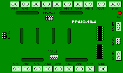
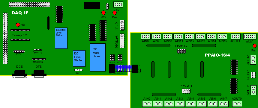
PPAIO-16/4
16-Channel analog input and 4-channel analog output
High-resolution image shot with a Canon EOS 5D MII
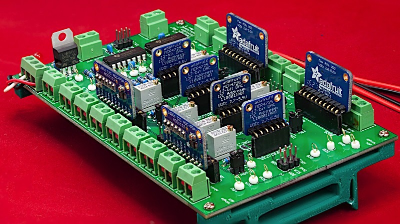
The PPAIO-16/4 board is an analog I/O board offering the following features:
- Open Source/Open Hardware design (Creative Commons 4.0 license)
- Single 5V power supply
- LED indicates when power is applied
- 16 single-ended analog inputs (15 bits resolution on single-ended inputs)
- or 8 differential (doubled-ended) inputs (16 bits resolution on differential inputs)
- Several different gain settings allow input voltages in the range 0 to 0.256V, 0 to 0.512V, 0 to 1.024V, 0 to 2.048V, 0 to 4.096V, and 0-5V
- Four 12-bit analog outputs
- Built-in amplifier circuitry for DAC outputs producing -5V to +5V or -10V to +10V outputs
- Span and zero pots for all four analog outputs
- I2C interface to DAQ IF board (using the DAQ standard 6-pin dual I2C interface connector)
- Test pins for all I2C signals and other signals
- Up to 2 PPAIO-16/4 boards may be daisy-chained off a single DAQ_IF I2C header providing up to 32 analog inputs and 8 analog outputs
- Optional DIN rail brackets allow installation on 35mm DIN rails
- DIN rail brackets are available in .STL format for 3D-printing
- Electrically-isolated inputs are possible using companion PPAC4 board
- 4-20mA inputs are possible using the PPAC420 board
- Full documentation including System Requirements Specifications (SyRS), Hardware Requirements Specifications (HRS), Hardware Inspection list (HI), Hardware Test Cases (HTC), Hardware Test Procedures (HTP), Hardware Design Description (HDD), and (reverse) Traceability Matrix (RTM) are available for the DAQ system, including this board.
Bill of Materials (BOM) for the PPAIO-16/4 board:
- (1) 5mm LED
- (1) 390 Ω 1/4-watt 1% resistor
- (20) 2-pin screw terminal (5mm/0.2" centers)
- (1) 3-pin screw terminal (5mm/0.2" centers)
- (2) 6-pin (2x3) male headers (ribbon cable connectors)
- (2) 8-pin (2x4) headers
- (4) 2-pin headers & jumpers
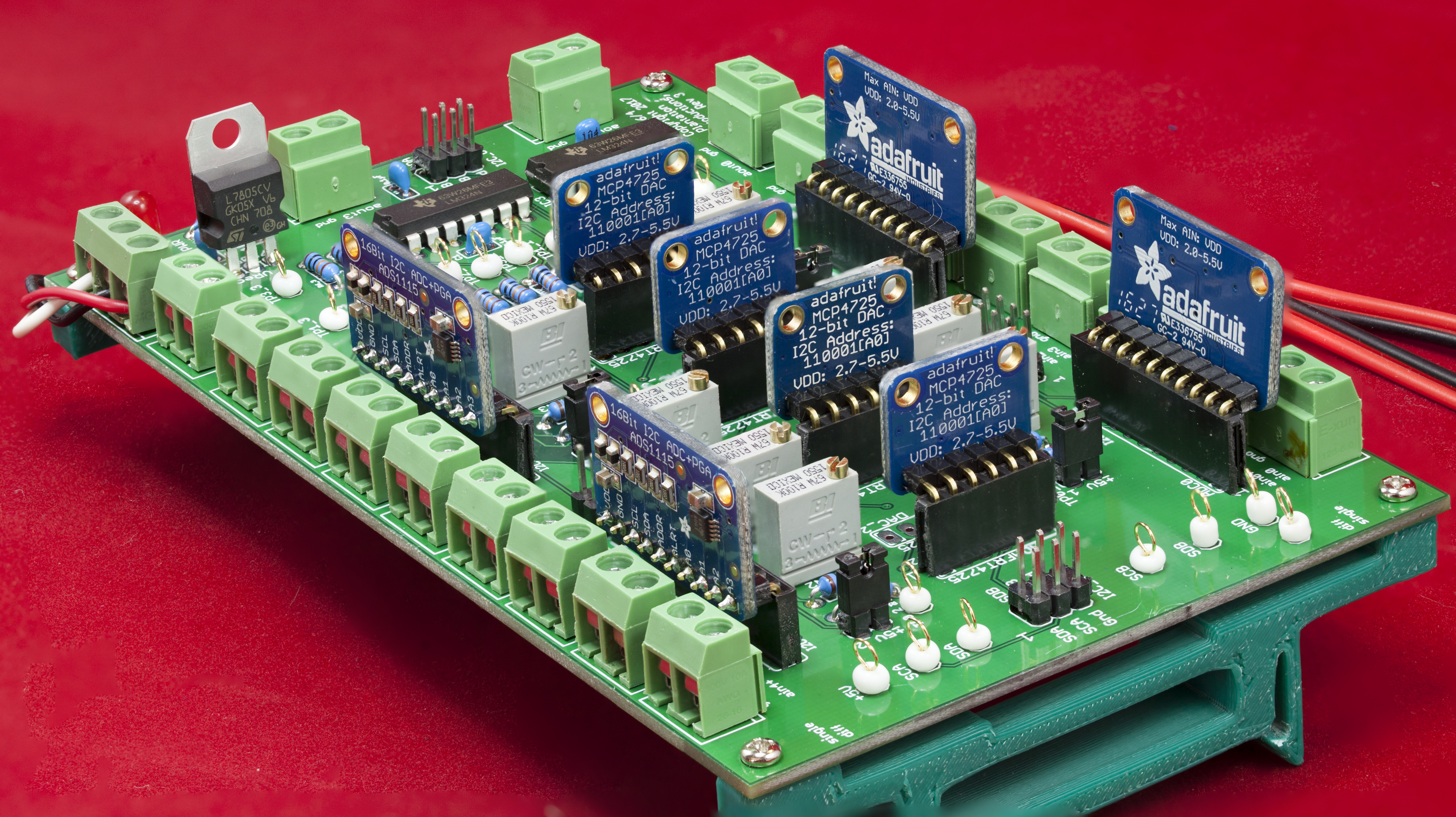
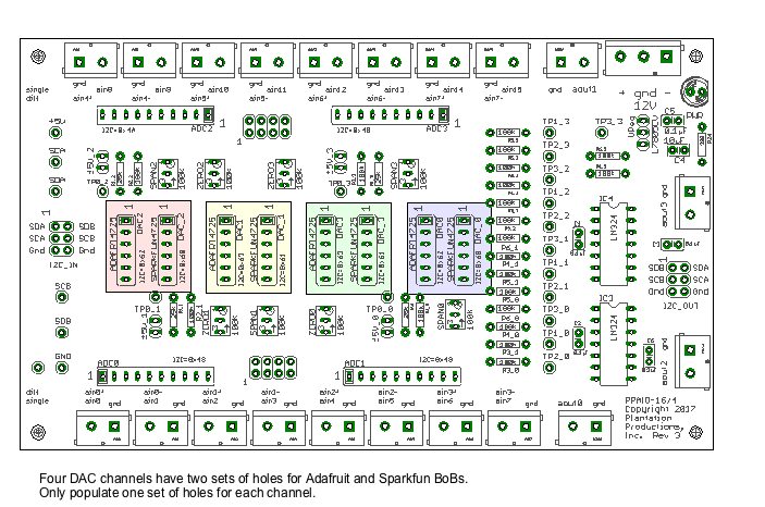
- (4) Adafruit ADS1115 ADC breakout boards w/right angle headers
- (4) Adafruit MCP4725 DAC breakout boards w/right angle headers OR (4) Sparkfun 4725 DAC breakout boards w/right angle headers
- (2) LM324 quad opamps
- (1) L7805CV 5V voltage regulator
- (5) 0.1 µF decoupling capacitors
- (1) 10 µF capacitor
- (3) 100 kΩ PCB trim pots (BI 67W R100K)
- (20) 100 kΩ 1% resistors
- (4) 25kΩ 1% resistors (or any close value)
- (1) PPAIPO-16/4 PCB
- Optional: (22) test pins
- Optional: one set of horizontal 35mm DIN rail mounts for DAQ boards
Note: If you only want a few PPAIO-16/4 PCBs, contact Plantation Productions (randy@plantation-productions.com) to see if there are any in stock. Bare boards are $25 each plus shipping; fully assembled and tested boards are $499 each. If you need more than a couple PCBs and you're not in a huge hurry, it costs about $150 (plus about 4-6 weeks) to have a set of 10 manufactured and shipped to you from China. I use Seeed Studio Fusion PCD service (https://www.seeedstudio.com/fusion.html). The PPDIO96 PCBs are four-layer boards. Here are the Gerber files for them (provide these files to Seeed Studio or your personal PCB manufacturer).
PPAIO-16/4 Gerber Files for PCB
If you want to modify or enhance the PPAIO-16/4 design, or re-layout the PCB using Eagle, here are the Eagle files:
PPAIO-16/4 Eagle files (Schematic and board layout)
If you simply want to view the schematic on-line, you'll find that here:
The DIN rails were created using AutoDesk's Fusion 360 (to produce STL files) and I personally print the results on a Lulzbot Taz6 3D printer using ABS filament (ABS is recommended for this job, PLA and PETG are a bit brittle). The STL files can be found here:
PP Standard DIN Rail Brackets 3D printer files
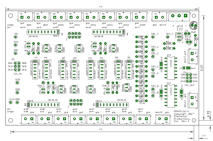
PPAIO-16/4 Board Layout
Connecting a PPAIO-16/4 board to a DAQ System
Up to eight PPDIO96 boards can be connected to a single DAQ_IF board. On the PPAIO-16/4 board there is an I2C_IN input header/connector and an I2C_out output header/connector. You may directly connect up to four boards to the four I2C headers on the DAQ_IF board; if you are using the standard Netburner firmware, you'll want to connect the first four PPAIO-16/4 boards as follows:
- First board connects to the DAQ_IF I2C_0_1 header
- Second board connects to the DAQ_IF I2C_2_3 header
- Third board connects to the DAQ_IF I2C_4_5 header
- Fourth board connects to the DAQ_IF I2C_6_7 header
Important! The first four boards must all have Adafruit 4725 DAC breakout boards (BoBs) installed (not Sparkfun BoBs).
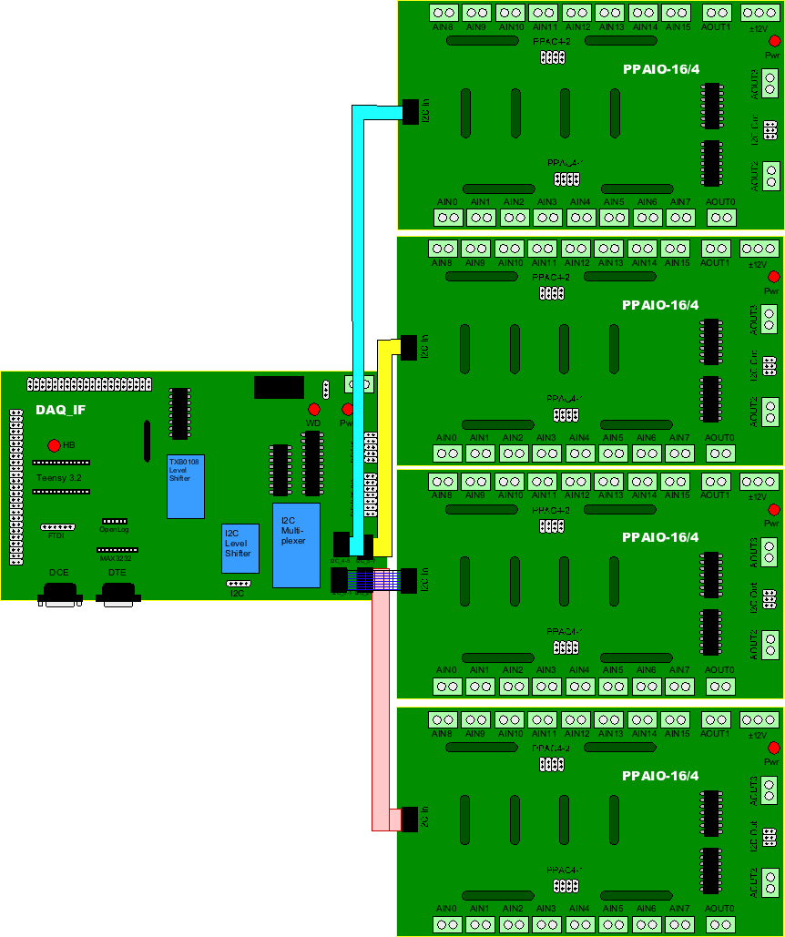
To add up to four additional PPAIO-16/4 boards to the system, you daisy-chain the next four boards off the first four boards:
(this diagram doesn't show the three boards attached to the remaining I2C ports on the DAQ_IF board; however, the firmware expects you to fill up the four connectors before doing any daisy-chaining.)
Important! The second set of four boards must all have Sparkfun 4725 DAC BoBs installed (not Adafruit BoBs).
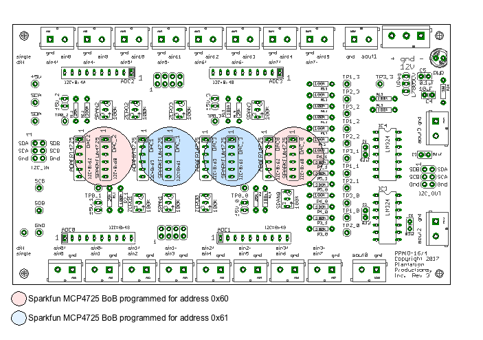
Each Adafruit and Sparkfun MCP4725 BoBs can respond to only one of two I2C addresses. The Sparkfun BoBs respond to addresses 0x60 and 0x61 while the Adafruit BoBs respond to I2C addresses 0x62 and 0x63. As each I2C connector on the PPAIO-16/4 boards supports two I2C busses, you can have four Adafruit or four Sparkfun BoBs on the same PPAIO-16/4.
The standard DAQ firmware (for the Netburner MOD54415 evaluation board) assumes that the first four boards in the system will contain Adafruit DACs and the second set of four boards (if present) will have Sparkfun DACs. This was a design choice made when writing the software to help reduce parts stocking issues. Most DAQ systems will not have more than four boards present in the system. Whenever you daisy-chain a pair of PPAIO-16/4 boards, one board must have Adafruit DACs and the other board must have Sparkfun DACs. By designing the software to query the daisy-chained boards only after querying all the directly connected boards, it was possible to get all the ADC and DAC boards from the same vendor (Adafruit) if you need less than four PPAIO-16/4 boards. In theory (if you're willing to change the firmware) there is no reason you couldn't daisy-chain first and fill up I2C ports after daisy-chaining. You could even put a pair of Sparkfun and a pair of Adafruit DACs on the same PPAIO-16/4 board (if you know what you are doing). However, the current software tries to avoid these situations in order to use a single vendor for the parts (e.g., to reduce shipping costs).
Note: there are two independent I2C busses on each 6-pin I2C header on the DAQ_IF board. The PPAIO-16/4 board swaps these two busses when the signal travels from the I2C In to the I2C Out connectors.Therefore, the first board uses the first I2C bus (for the ADCs, the DACs use both busses) and the second board uses the second I2C bus. Therefore, under no circumstances should you attempt to daisy-chain more than two PPAIO-16/4 boards; the third board would wind up sitting on the same bus as the first board and you would get address conflicts.
Selecting an I2C Bus on the DAQ IF Board (Selecting a PPAIO-16/4 Board)
The four 6-pin I2C headers on the DAQ IF board contain two independent I2C busses. This means that there are a total of 8 I2C busses present. The DAQ IF board only requires a single I2C bus from the single-board computer module (e.g., the Netburner MOD54415). It creates a set of eight I2C busses via the use of an Adafruit TCA9584 BoB. The Adafruit TCA9584 I2C multiplexor BoB responds to I2C address 0x70. If you write a zero to this address, the TCA9584 chip will disable all eight busses. If you write a value containing a single '1' bit to this address (0x01, 0x02, 0x04, 0x08, 0x10, 0x20, 0x40, or 0x80) then the TCA9584 will activate the specified bus (0-7) for all future I2C operations until a new value is written to I2C address 0x70.
You can find the data sheet for the TCA9584 here
Note that if you are using the standard firmware (Netburner code) then you don't have to worry about controlling the multiplexor; the standard firmware handles all that for you.
Digital-to-Analog Conversion on the PPAIO-16/4
The PPAIO-16/4 contains four digital-to-analog converters (DACs). The DACs breakout boards (Adafruit and Sparkfun, as noted above). The BoBs both contain an MCP4725 DAC chip and appropriate interface components. The BoBs from the two vendors are not pin compatible; the Adafruit BoB brings out an address selection pin to the header,the Sparkfun BoB uses a cut/jump on the PCB to select the address (so it has one less pin than the Adafruit BoB) Therefore, there are two sets of holes for each DAC channel on the PPAIO-16/4. You cannot install BoBs in both sets of holes for a single channel -- the signals from each board would interfere with one another.
As noted in the previous section, you should install only Adafruit or Sparkfun DAC BoBs on a single PPAIO-16/4 board (do not mix and match them). If you install Adafruit BoBs, the PPAIO-16/4 circuit board will automatically select the appropriate I2C addresses for you (by shorting the address pin to ground or tying it to +5V). If you install Sparkfun BoBs on the PPAIO-16/4 then you will have to ensure that the correct address is selected on the Sparkfun BoB. Address selection on the Sparkfun BoB is handled by a set of solder pads on the BoB:
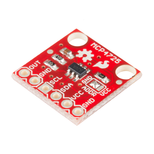
If the solder bridge is across the middle and left (Gnd) pads, then the BoB responds to address 0x60; if the solder bridge is across the middle and right (VCC) pads, then the Bob responds to address 0x61. By default, the Sparkfun Bob ships with address 0x60 selected (Gnd pad selected). To make the BoB respond to address 0x61 you must unsolder the Gnd/middle pad connection and create a solder bridge across the middle/Vcc pads.
The (Sparkfun version of the) PPAIO-16/4 requires a total of four Sparkfun MCP4725 BoBs: two at address 0x60 and two at address 0x61.
The PPAIO-16/4 board refers to the two incoming I2C busses as "A" and "B" (SDA/SCA and SDB/SCB). If the PPAIO-16/4 is connected directly to a DAQ IF board, then the "A" bus is the first I2C bus of the pair and the "B" bus is the second I2C bus of the pair (e.g., if the PPAIO-16/4 is connected to the I2C_0_1 header then the "A" bus is I2C bus zero and the "B" bus is I2C bus one). If the PPAIO-16/4 is daisy-chained to another PPAIO-16/4 board, then the two busses are swapped (e.g., "A" bus would be I2C bus one and "B" bus would be I2C bus zero in this example).
The MCP4725 DAC chip (used on the Adafruit and Sparkfun BoBs) produces a 0 to 5V output based on a 12-bit unsigned integer programmed into the chip. For MCP4725 programming details, please consult the MCP4725 data sheet.
For many applications, the 0-5V range is insufficient. Therefore, the PPAIO-16/4 board contains a set of analog amplifiers to boost this range to ±5V or ±10V (jumper selectable for each DAC channel).

The PPAIO-16/4 board also contains SPAN (gain) and ZERO (offset) potentiometers to allow you to precisely calibrate the outputs.
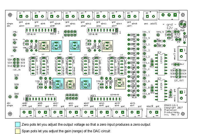
There is a ZERO and a SPAN pot for each channel. You must calibrate the PPAIO-16/4 DAC channels before use. To roughtly calibrate the DAC channels you repeat the following steps:
- Program the MCP4725 to produce 0V output (write 0x0 to the chip) for a given channel
- Adjust the ZERO pot for that channel until the corresponding AOUTx connector shows -5V (or -10V if the channel's voltage select jumper is removed)
- Program the MCP4725 to produce 5V output (write 0xFFF to the chip)
- Adjust the SPAN pot for that channel until the corresponding AOUTx connector shows +5V (or +10V if the channel's voltage select jumper is removed)
Note: the SPAN and ZERO functions are not completely independent. Adjusting one pot will likely affect the other value. Therefore, you will need to repeat the above steps several times to get consistent results (3-4 times should be a good start). Also, you should do an initial calibration with the voltage selection jumpers installed (producing ±5V output). ±10V is close enough to the opamp "rails" that you might get clipping if you exceed an allowable span/zero combination. By doing an initial calibration to ±5V you have lots of headroom to play with. Once you've calibrated the output to ±5V, you can quickly (typically in one or two steps) recalibrate for ±10V.
Once you've roughly calibrated the system using the above steps, you should finish the calibration using the following steps:
- Program the MCP4725 to produce 2.5V output (write 0x800 to the chip) for a given channel
- Adjust the ZERO pot for that channel until the corresponding AOUTx connector shows 0V
- Program the MCP4725 to produce 0V output (write 0x0 to the chip) for a given channel
- Adjust SPAN and ZERO to produce -5V (or -10V) on the output
- Program the MCP4725 to produce 5V output (write 0xFFF to the chip)
- Adjust the SPAN pot for that channel until the corresponding AOUTx connector shows +5V (or +10V if the channel's voltage select jumper is removed)
Repeat the above steps until you get a satisfactory result. Note that most systems can tolerate a little inaccuracy on either end (-5V/+5V or -10V/+10V) but you really should try to get the 0V point set as tightly as possible (when the MCP4725 is programmed to produce 2.5V as output).
Analog-to-Digital Conversion on the PPAIO-16/4
The PPAIO-16/4 contains four analog converter modules (ADCs). Each ADC module (Adafruit ADS1115 BoB) supports four multiplexed channels of analog input (single-ended, two channels of differential analog input). The ADS1115 IC responds to one of four separate I2C addresses (0x48, 0x49, 0x4a, 0x4b) by tying the single address pin to one of four other pins (Vcc, Gnd, SDA, or SCL). Because the Adafruit brings this address signal out to a header pin, the PPAIO-16/4 PCB automatically selects the appropriate address for each BoB. For more details on ADS1115 addressing, please consult the data sheet:
The ADS1115 performs a signed analog conversion. However, the input pins on the ADS1115 must never go negative. Therefore, when operating in single-ended mode the ADS1115 can only handle non-negative voltages. This effectively limits the conversion to 15 bits (as the 16th bit, the sign bit, will always be zero). To produce negative results you must use the ADS1115 in differential mode. Differential mode combines two inputs and produces a value that is the difference between the two inputs. Both inputs must be non-negative, but if the second input is greater than the first input, their difference is a negative number. Therefore, the only way to get a full 16-bit precision out of the ADS1115 is to use differential mode. Note that the DAQ system PPAC4 (analog conditioning) board accepts ±10V and produces a differential signal compatible with the ADS1115.
The ADS1115 provides a programmable gain amplifier (PGA) that can amplify small voltage signals for use by the later ADC stage. The ADS1115 supports the following gain ranges:
- 0 to 0.255V
- 0 to 0.511V
- 0 to 1.023V
- 0 to 2.047V
- 0 to 4.095V
- 0 to 5V/6.144V
Note that the input voltage must not exceed Vcc (nominally 5V) plus 0.3V. The last gain range is actually 0 to 6.144V (to produce a full-range 15-bit result of 0x7FFF/32767). However, as the ADS1115 on the PPAIO-16/4 board is powered by +5V, the input voltage cannot exceed +5V. Therefore, in the largest gain range the ADC will produce values in the range 0 to 26,667 for input voltages in the range 0 to 5V.
When operating in differential mode the ADS1115 converts the difference in voltage between a pair of pins to a signed 16-bit value. On the PPAIO-16/4 board, the differential pairs are always the following:
- AIN0d = AIN0(+) and AIN1(-), result = AIN0 - AIN1
- AIN1d = AIN2(+) and AIN3(-), result = AIN2 - AIN3
- AIN2d = AIN4(+) and AIN5(-), result = AIN4 - AIN5
- AIN3d = AIN6(+) and AIN7(-), result = AIN6 - AIN7
- AIN4d = AIN8(+) and AIN9(-), result = AIN8 - AIN9
- AIN5d = AIN10(+) and AIN11(-), result = AIN10 - AIN11
- AIN6d = AIN12(+) and AIN13(-), result = AIN12 - AIN13
- AIN7d = AIN14(+) and AIN15(-), result = AIN14 - AIN15
Note that in differitial mode the input voltages on both pins are limited to the same range (specified by the PGA) as in single-ended mode. E.g., if the PGA is set to the range 0 to 4.095V then the differential input pin voltages must not exceed this range.
Pairing a PPAIO-16/4 With a PPAC4 Analog Conditioning Module
The PPAC4 analog conditioning module converts voltages in the range ±10V to a differential signal that is compatible with the ADS1115 differential inputs. The PPAC4 also contains four isolation amplifiers that isolate the incoming analog signals from each other and isolate those signals from the PPAIO-16/4 and DAQ system circuitry. For this reason alone (isolation) it is a good idea to use PPAC4 modules to protect DAQ system electronics and to protect the analog sources from one another.
The PPAC4 produces a differential signal whose voltages are in the range 0 to 4.095V. Therefore, by selecting the PGA gain of 0 to 4.095V the PPAC4 module allows you to take full advantage of the ADS1115 16-bit range.
There are two ways to connect a PPAC4 board to a PPAIO-16/4 board:
- Directly wire the AOUT +/- pins on the PPAC4 to the corresponding AIN connectors on the PPAIO-16/4 board
- Use a ribbon cable to connect the four channels on the PPAC4 board to four differential inputs on the PPAIO-16/4 board
Using an 8-conductor (2x4 header) ribbon cable is definitely more convenient. If noise is an issue, direct wiring may producing a cleaner signal. Using the ribbon cable approach is also less flexible -- with a ribbon cable you can only attach the PPAC4 to (AIN0d, AIN1d, AIN2d, AIN3d) or (AIN4d, AIN5d, AIN6d, AIN7d). You could not, for example, connect to (AIN0d, AIN3D, AIN4, AIN7d) using a ribbon cable. However, you can connect the PPAC4 to any four diffierential pairs using direct wiring.
For more details on the PPAC4, check out the PPAC4 web page
Pairing a PPAIO-16/4 With a PPAC420 and PPAC4 Analog Conditioning Modules
The PPAC420 analog conditioning module converts a 4-20mA current loop to a voltage in the range -1.25V to +5V (it actually converts currents in the range 0 mA to 4mA to a voltage in the range -1.25V to 0V and currents in the range 4mA to 20 mA to voltages in the range 0V to +5V). Because the PPAC420 can produce negative voltages you cannot feed its output directly into a PPAIO-16/4 analog input. You must feed the PPAC420 output to a PPAC4 input and then feed the corresponding differential output to the PPAIO-16/4 board.
Because the PPAC420 board converts the 0-20mA input to a voltage in the range -1.25 to +5V, you wind up using only half the range possible with the PPAIO-16/4 ADC input (assuming you're using the standard 0 to 4.095V gain range for the PPAC4). As a result, you lose one bit of precision. If you really want that extra bit back, you can always program the ADS1115 chip to use the 0 to 2.047V gain range. Just be sure to carefully calibrate the PPAC4 output so that it doesn't exceed 2.047V when feeding the PPAC420 20mA.
For more details on the PPAC420, check out the PPAC420 web page
Programming PPAIO-16/4
Note: some of this code was adapted from the Adafruit and Sparkfun Arduino-compatible libraries for the MCP4725 and ADS1115 devices. This particular code was written to run on a Teensy 3.2 installed on a DAQ IF board. For comparable examples using the Netburner, please see the standard firmware source code. The following source code is written for the Teensy 3.2 using the Arduino IDE with appropriate extensions for the Teensy. See the Teensy homepage for more details. Note that this source code makes use of the Adafruit libraries for the MCP4725 and ADS1115; you can find the code for those libraries at https://learn.adafruit.com/adafruit-4-channel-adc-breakouts/overview and https://learn.adafruit.com/mcp4725-12-bit-dac-tutorial/overview.
To begin with, let's get some declarative stuff out of the way.
#include <SPI.h>
#include <Wire.h>
#include <Adafruit_MCP4725.h>
#include <Adafruit_ADS1015.h>

#define ppdio96_IC2     2
#define ppdio96_IC3     3
#define ppdio96_IC4     4
#define ppdio96_IC5     5
#define ppdio96_IC6     6
#define ppdio96_IC7     7

#define spics           10
#define mosi            11
#define miso            12
#define spiclk          13
#define led             spiclk

#define a0              14
#define a1              15
#define a2              16
#define wd_rfsh         17
#define wd_latch        20
#define j2_38           21
#define IRQ             22
#define reset           23


#define isAdafruitDAC   1
//#define isSparkFunDAC 1

const   double  maxErrVal   = 0.175;


Adafruit_MCP4725 dac62;
Adafruit_MCP4725 dac63;

Adafruit_ADS1115 adse0(0x48);  /* Use this for the 16-bit version */
Adafruit_ADS1115 adse1(0x49);  /* Use this for the 16-bit version */
Adafruit_ADS1115 adse2(0x4a);  /* Use this for the 16-bit version */
Adafruit_ADS1115 adse3(0x4b);  /* Use this for the 16-bit version */
Adafruit_ADS1115 *adse[4] = { &adse0, &adse1, &adse2, &adse3 };


// These functions reset the WD timer and refresh it. This prevents
// annoying watchdog timer timeouts during the execution of the test code

void toggleReset( void )
{
    digitalWrite( reset, 0 );
    delay( 3 );
    digitalWrite( reset, 1 );
    delay( 3 );
}

void refreshWD( void )
{
    digitalWrite(wd_rfsh, HIGH );
    delayMicroseconds( 10 );
    digitalWrite( wd_rfsh, LOW);
    delayMicroseconds( 10 );
}
Next, let's look at some code to program the TCA9548 I2C expansion chip. The "setI2Cbus" function expects a single parameter in the range 0 to 7 and it activates the corresonding I2C bus on the DAQ IF board. Note that if you pass a value outside the range 0 to 7 this code will disable all I2C busses on the TCA9548 expander. So passing "-1" as the argument is a good way to disable the 8 expansion I2C busses on the DAQ IF.
// Program the TCA9548 I2C expander chip
// Write a one bit in the bit position corresponding
// to the bus you want active.

void setI2Cbus( int bus )
{
    uint8_t bits = 0;

    switch( bus )
    {
        case 0:
            bits = 1;
            break;

        case 1:
            bits = 2;
            break;

        case 2:
            bits = 4;
            break;

        case 3:
            bits = 8;
            break;

        case 4:
            bits = 0x10;
            break;

        case 5:
            bits = 0x20;
            break;

        case 6:
            bits = 0x40;
            break;

        case 7:
            bits = 0x80;
            break;

        default:
            bits = 0;
    }
    Wire.beginTransmission( 0x70 );
    Wire.send( bits );
    Wire.endTransmission();

} // setI2Cbus


Here's the setup function that initializes the chips (and other stuff)
void setup()
{
    Serial.begin(9600);
    Wire.begin();

    pinMode(wd_latch, INPUT);

    pinMode( IRQ, INPUT );
    pinMode( wd_rfsh, OUTPUT );
    pinMode( wd_latch, INPUT );
    pinMode( reset, OUTPUT );
    pinMode(a0, OUTPUT);
    pinMode(a1, OUTPUT);
    pinMode(a2, OUTPUT);
    pinMode(spics, OUTPUT);

    refreshWD();
    toggleReset();
    refreshWD();

    // For Adafruit MCP4725A1 the address is 0x62 (default) or 0x63 (ADDR pin tied to VCC)
    // For SparkFun MCP4725A0 the address is 0x60 or 0x61
    // For MCP4725A2 the address is 0x64 or 0x65

    #ifdef isAdafruitDAC

        dac62.begin(0x62);      // AOUT0 & AOUT2
        dac63.begin(0x63);      // AOUT1 & AOUT3

    #elif isSparkFunDAC

        dac62.begin(0x60);      // AOUT0 & AOUT2
        dac63.begin(0x61);      // AOUT1 & AOUT3

    #endif

    // The ADC input range (or gain) can be changed via the following
    // functions, but be careful never to exceed VDD +0.3V max, or to
    // exceed the upper and lower limits if you adjust the input range!
    // Setting these values incorrectly may destroy your ADC!
    //                                                                ADS1015  ADS1115
    //                                                                -------  -------
    // ads.setGain(GAIN_TWOTHIRDS);  // 2/3x gain +/- 6.144V  1 bit = 3mV      0.1875mV (default)
    // ads.setGain(GAIN_ONE);        // 1x gain   +/- 4.096V  1 bit = 2mV      0.125mV
    // ads.setGain(GAIN_TWO);        // 2x gain   +/- 2.048V  1 bit = 1mV      0.0625mV
    // ads.setGain(GAIN_FOUR);       // 4x gain   +/- 1.024V  1 bit = 0.5mV    0.03125mV
    // ads.setGain(GAIN_EIGHT);      // 8x gain   +/- 0.512V  1 bit = 0.25mV   0.015625mV
    // ads.setGain(GAIN_SIXTEEN);    // 16x gain  +/- 0.256V  1 bit = 0.125mV  0.0078125mV

    adse0.begin();
    adse0.setGain( GAIN_TWOTHIRDS );

    adse1.begin();
    adse1.setGain( GAIN_TWOTHIRDS );

    adse2.begin();
    adse2.setGain( GAIN_TWOTHIRDS );

    adse3.begin();
    adse3.setGain( GAIN_TWOTHIRDS );


    Serial.println( "PPAIO test procedure" );

    delay( 2000 );

}
And here's the "loop" function that reads ADCs and writes DACs:
void loop()
{

	// Write to Adafruit DACs 0 & 1:

	setI2Cbus( 0 );

	dac62.setVoltage( 0, false );
	dac62.setVoltage( 4095, false );

	dac63.setVoltage( 0, false );
	dac63.setVoltage( 4095, false );


	// Write to Adafruit DACs 2 & 3:

	setI2Cbus( 1 );

	dac62.setVoltage( 0, false );
	dac62.setVoltage( 4095, false );

	dac63.setVoltage( 0, false );
	dac63.setVoltage( 4095, false );

	// Read the ADCs. They are all on bus 0:

    setI2Cbus( 0 );
    for( int i=0; i < 1; ++i )
    {
        for( int ch = 0; ch < 1; ++ch )
        {
            uint16_t result;

            result  = adse[i]->readADC_SingleEnded( ch );
            Serial.printf( " >%d:%d = ", i, ch );
            Serial.print( result );
        }
    }
    Serial.println();

}