
Note: All photographs appearing on this page are freely usable for any purpose. Links to high-resolution versions of the pictures appear below each picture.
Digital Data Acquisition & Control System
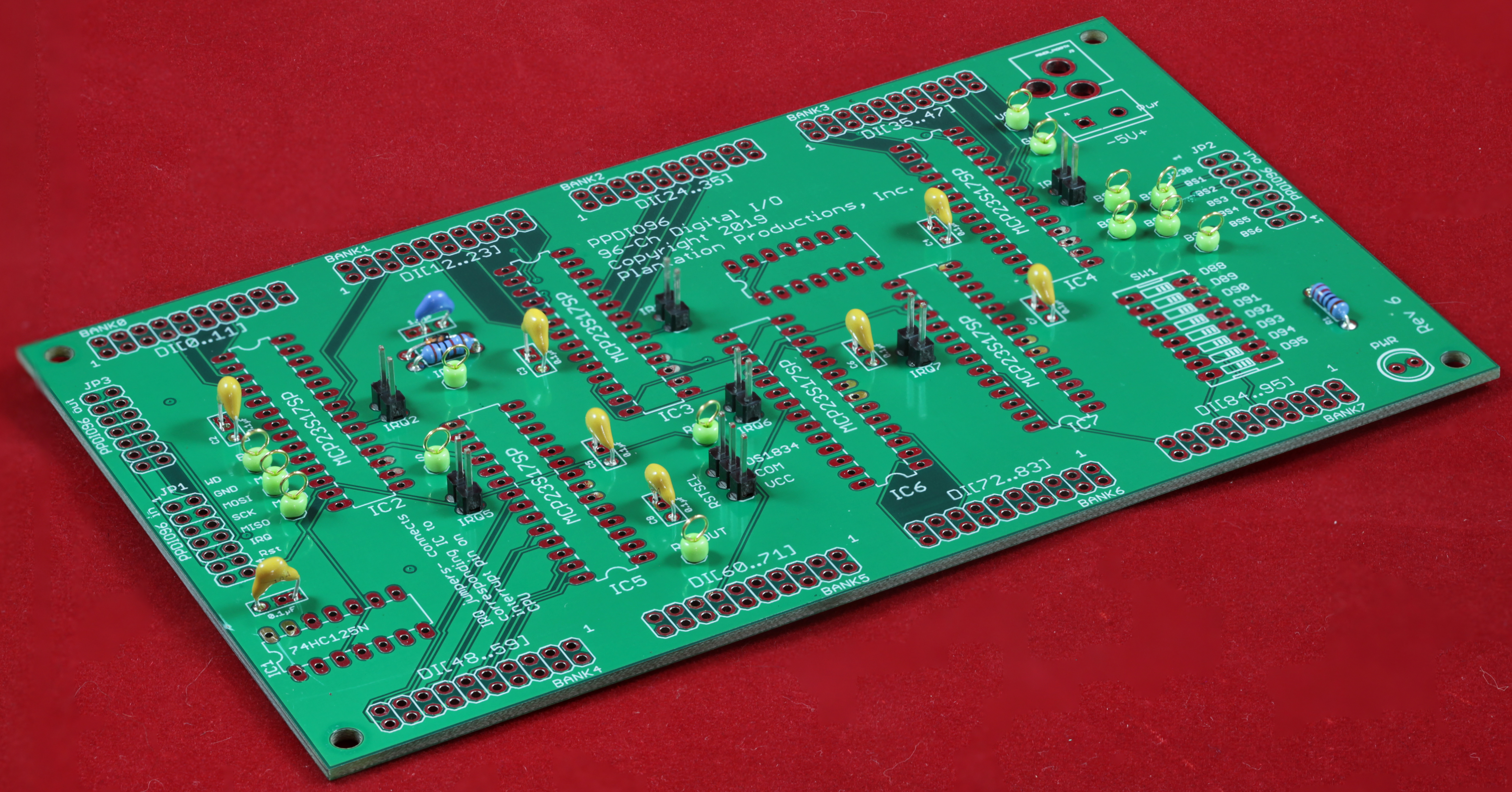
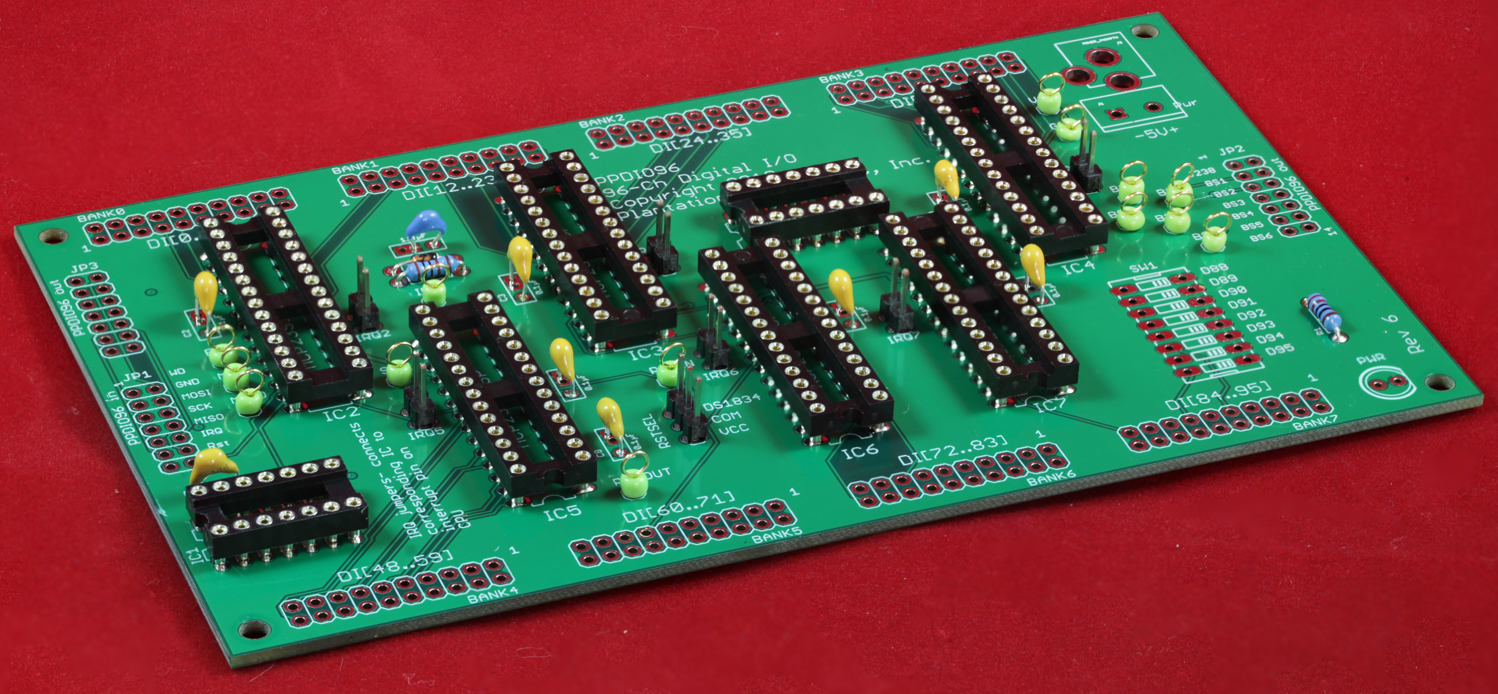
PPDIO96
96-Channel digital I/O board

High-resolution image shot with a Canon EOS 5D MII

The PPDIO96 board is a 96-channel digital I/O board. The PPDIO96 offers the following features:
- Open Source/Open Hardware design (Creative Commons 4.0 license)
- Single 5V power supply
- LED indicates when power is applied
- 96 independent input or output bits (data direction of each pin is programmable)
- 5V/TTL-level logic on each pin
- Up to 25 mA (sink or source) current on each I/O pin (note: it would be unwise to try and sink or source 25 mA on all I/O pins simultaneously -- that would be 2.5A on the I/O pins alone)
- 8-position DIP switch connected to bits 88-95 (may be disabled by moving all switches to the off position)
- Fast SPI bus operation utilizing high-performance MCP23S17 general-purpose I/O expander chips
- Test pins for all SPI signals, IRQ pin, and other signals
- Optional programmable pull-up resistors on each input pin allows dry contact connections
- Programmable polarity on all input pins (active low or active high)
- Utilizes only a single SPI chip select line for all 96 I/O bits (plus three data I/O lines to drive a 74HC138 demultiplexor)
- Supports interrupt driven operation, selectable on a chip-by-chip (16 I/O lines per chip) basis
- 96 I/O pins divided up into 8 banks of 12 bits each
- Fully buffered -- presents only a single TTL load on the SPI bus and chip select lines
- Reset and Watchdog timeout signals place all I/O expander chips in fail-safe mode (all pins programmed as inputs)
- Noise filtering on reset line to prevent noise transients from resetting the board
- Up to 6 PPDIO96 boards may be daisy-chained off a single DAQ_IF board providing up to 576 bits of digital I/O
- Optional DIN rail brackets allow installation on 35mm DIN rails
- DIN rail brackets are available in .STL format for 3D-printing
- Optically-isolated inputs are possible using companion PPOpto-12 board
- Each bank of 12 I/O pins can be brought out to screw terminals using the PPBreakout board or PPBreakin board
- Full documentation including System Requirements Specifications (SyRS), Hardware Requirements Specifications (HRS), Hardware Inspection list (HI), Hardware Test Cases (HTC), Hardware Test Procedures (HTP), Hardware Design Description (HDD), and (reverse) Traceability Matrix (RTM) are available for the DAQ system, including this board.
Bill of Materials (BOM) for the PPDIO96 board:
- (1) 5mm LED
- (1) 220 Ω 1/4-watt 1% resistor
- (2) 20 kΩ 1/4-watt 1% resistor
- (1) 1N4148 diode
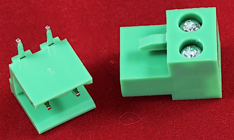
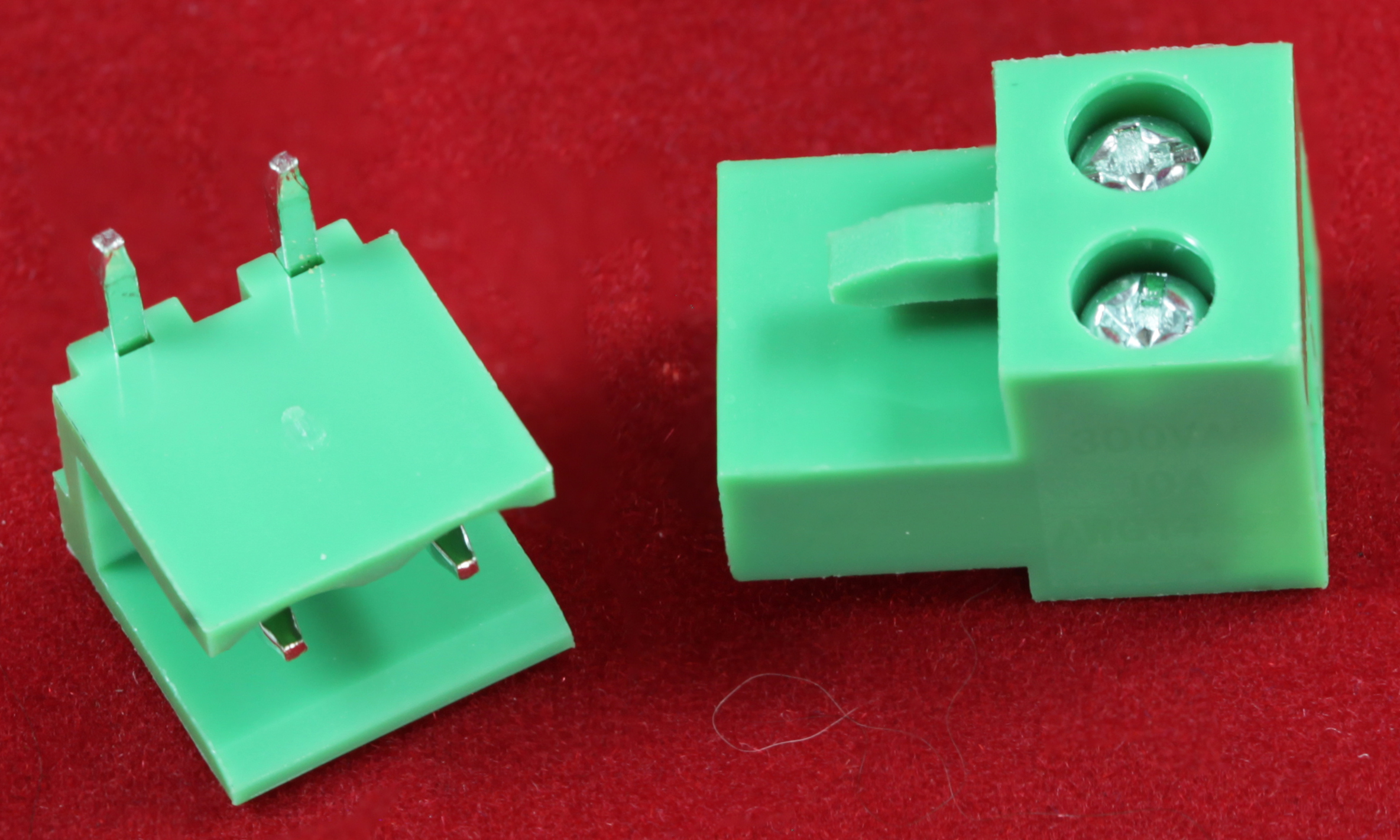
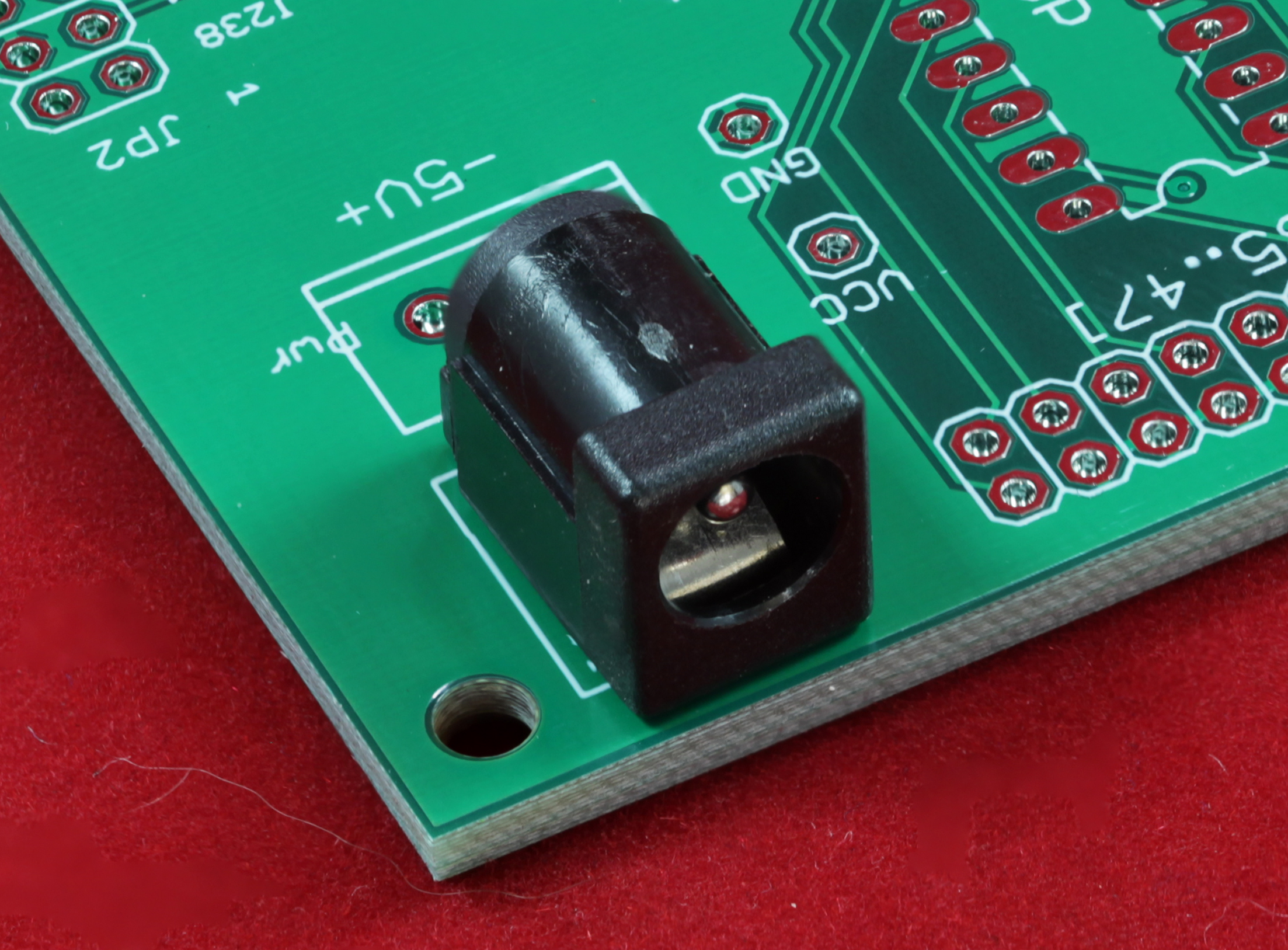
- (1) 2-pin screw terminal (5mm/0.2" centers) or (1) 5.5mm Barrel Jack for power
- (8) 20-pin (2x10) male headers (ribbon cable connectors)
- (3) 14-pin (2x7) male headers (SPI-6 bus)
- (6) 2-pin headers (for jumpers)
- Optional: (6) 2-pin jumpers
- (6) MCP23S17 ICs
- (1) 74HC125 quad tri-state buffer
- (8) 0.1 µF decoupling capacitors
- (1) 1.0 µF capacitor (timing)
- (1) 8-position DIP switch
- (1) PPDIO96 PCB
- Optional: (14) test pins
- Optional: one set of horizontal 35mm DIN rail mounts for DAQ boards
- Optional: one PPOPTO vertical 35mm DIN rail mount
Note: If you only want a few PPDIO96 PCBs, contact Plantation Productions (randy@plantation-productions.com) to see if there are any in stock. Bare boards are $25 each plus shipping; fully assembled and tested boards are $499 each. If you need more than a couple PCBs and you're not in a huge hurry, it costs about $150 (plus about 4-6 weeks) to have a set of 10 manufactured and shipped to you from China. I use Seeed Studio Fusion PCD service (https://www.seeedstudio.com/fusion.html). The PPDIO96 PCBs are four-layer boards. Here are the Gerber files for them (provide these files to Seeed Studio or your personal PCB manufacturer).
If you want to modify or enhance the PPDIO96 design, or re-layout the PCB using Eagle, here are the Eagle files:
PPDIO96 Eagle files (Schematic and board layout)
If you simply want to view the schematic on-line, you'll find that here:
The DIN rails were created using AutoDesk's Fusion 360 (to produce STL files) and I personally print the results on a Lulzbot Taz6 3D printer using ABS filament (ABS is recommended for this job, PLA and PETG are a bit brittle). The STL files can be found here:
PP Standard DIN Rail Brackets 3D printer files
Revision History:
Revs 2/3: Changed various trace names; manually routed various signals to reduce noise; added second SPI-6 bus connector to make it more convenient to stack boards (vertically); tied certain 74hc125 enable lines to ground; modified decoupling capacitor layout to handle multiple capacitor sizes.
Rev4: Changed CS for IC2, 3, and 4 to 1, 2, and 3, respectively. This frees up selects 0 and 4 for use when initializing HAEN. Tied reset line high (relying on power-on reset) to prevent problems with noise on the reset line. Moved the power connector to support pluggable connector. Added 5.5mm Power Jack as an option.
Revs 5, 6, 7: Added delay circuit to require reset pulses at least 20 msec long (to filter out transient noise); added jumper to select reset source (Vcc or delay circuit); moved power LED away from board edge; added two reset test pins; Changed silk-screen text for SPI-6 bus and PPDIO banks; moved decoupling capacitor for 7414; added legend for 7414.
The biggest change to the board was the inclusion of a "debouncing circuit" for the reset line. In the field, relay noise was cause several sub-microsecond spikes on the reset line. This inadvertently reset the MCP23S17 creating some severe problems (e.g., SCRAMming a nuclear reactor). The new debounce circuit requires a reset pulse of about 20 milliseconds before the signal affects the MCP23S17 ICs. This time value is programmable by changing a resistor and capacitor on the PCB (1 µF capacitor and 20kΩ resistor). There is also a jump (RSTSET) that allows you to disable the reset function on the board (putting a jump between "COM" and "VCC" on the RSTSET header disables the chip reset function).
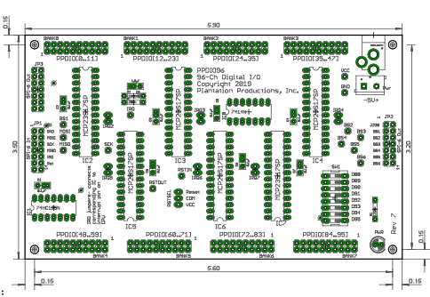
PPDIO96 Board Layout
Connecting a PPDIO96 board to a DAQ System
Up to six PPDIO96 boards can be daisy-chained to a single DAQ_IF board. On the PPDIO96 board there is a SPI-6 input header/connector and two SPI-6 output header connectors.
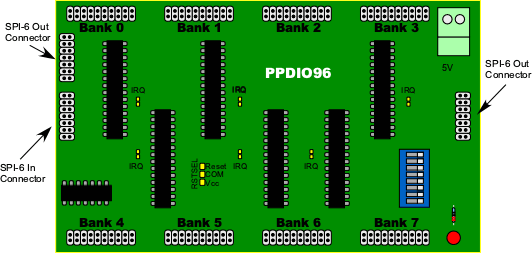
The SPI-6 In and SPI-6 Out headers have the following pinouts:

Note that the only difference between the two is that the BS1..BS6 lines have been shifted up one pin (BS1 is lost and Vcc is connected to pin 2 on the output connector). This shift allows each PPDIO96 board to be electrically identical yet respond to a different board select pin (BS1-BS6) based on their position in the daisy-chain.
To daisy-chain PPDIO96 boards (that is, form a bus of PPDIO96 boards), use the following wiring scheme:
- First PPDIO96 board in chain wires its SPI-6 input connector to the SPI-6 connector on the DAQ_IF board
- Second PPDIO96 board in chain wires its SPI-6 input connector to (either of) the output SPI-6 connectors on the first PPDIO96 board
- Third PPDIO96 board in chain wires its SPI-6 input connector to one of the output SPI-6 connectors on the second PPDIO96 board
- Fourth PPDIO96 board in chain wires its SPI-6 input connector to an output SPI-6 connector on the third PPDIO96 board
- Fifth PPDIO96 board in chain wires its SPI-6 input connector to an output SPI-6 connector on the fourth PPDIO96 board
- Sixth PPDIO96 board in chain wires its SPI-6 input connector to an output SPI-6 connector on the fifth PPDIO96 board
The last board in the daisy chain (including the situation where there are fewer than six boards connected together) leaves its SPI-6 output connectors disconnected.
Because the DAQ system sends hi-speed SPI signals through the SPI-6 bus connectors you should try to keep the (ribbon) cables connected the daisy-chained PPDIO96 boards as short as possible. Also try to avoid placing those cable near other high-frequency cables or cables that have large power spikes on them (to avoid inductive coupling with those other signals). The best cable arrangement is to place the boards end-to-end as close together as possible.

Connecting Digital Inputs to the PPDIO96 Board
The 96 I/O lines on the PPDIO96 are broken up into 8 banks of 12 bits/bank. Each bank has a pinout that is compatible with the PPOpto-12 and PPBreakout output connectors:

Note, however, that the bit numbers are offset according to the bank number:
| Bank # | Starting bit # |
|---|---|
0 |
D0 |
1 |
D12 |
2 |
D24 |
3 |
D36 |
4 |
D48 |
5 |
D60 |
6 |
D72 |
7 |
D84 |
So, for example, pins 19 and 20 for Bank 3 would actually be D36 and D37, respectively (and pins 1 and 2 would be D47 and D46, respectively).
Because the digital inputs to the PPDIO96 aren't usually high-frequency signals (host system generally poll these inputs at around 10-20 Hz), their cabling requirements aren't as critical as the SPI-6 in/out/bus connections.
The MCP23S17 GPIO expansion ICs used on the PPDIO96 run off a 5V power supply. Input pins expect a 5V/TTL-logic level. Either 3.3V or 5V logic as inputs will work just fine on the PPDIO96 input pins. Each pin can be programmed to provide an internal pull-up resistor (to +5V, though it is a weak pull-up) so you can use dry contact inputs as well. If you wish to connect any other voltage levels to the PPDIO96 you will need to provide a level shifter to accomplish this. One easy way to do this is to use a PPOpto-12 board that provide optical isolation and allows input voltages betwee 5VDC and 24VDC.
When using pins on the PPDIO96 as outputs, the PPDIO always produces 5V logic output values. If you need to control a higher or lower voltage you should use a level shifter circuit to achieve this. A mismatch between the PPDIO96 output voltage and some other device could damage the PPDIO96, the other device, or both.
DIP Switches on the PPDIO96
The PPDIO96 board contains eight DIP switches (in a single package) that connect to inputs D88 through D95. This provides a convenient set of switches for setting default values and other options within your software (by reading these DIP switches). The DIP switches connect the specified (input) pins to ground. To use these switches, you should program pins D88 through D95 as inputs and turn on the internal MCP23S17 pull-up resistors for those inputs. After this initialization, the system will read a closed switch as a '0' and an open switch as a '1'.
If you do not intend to use the DIP switches, you do not need to populate the DIP switch package on the board. If the DIP switch is already present and you don't want to use it, just make sure that the switches are all in the open position.
Warning: If a DIP switch is in the closed position and you program the corresponding MCP23S17 pin as an output, this will form a direct short to ground and may damage the MCP23S17 chip. If you program an MCP23S17 pin as an input and the corresponding DIP switch is closed, this will not damage the MCP23S17 but it could damage whatever device is providing the signal source. In the best case, having the switch closed will always force a read of zero, ignoring the actual input data. Moral of the story: when not use a DIP switch make sure it is in the open position; better yet, don't install the DIP switch package if you don't intend to use andy of the DIP switches. If the DIP switches are already installed (and you don't want to use them), it's probably best not to use I/O pins D88 through D95 on the PPDIO96 board.
Test Pins on the PPDIO96
The PPDIO96 board contains 12 test locations that make varous signals available to DVMs, Oscilloscopes, logic analyzers, and other devices. The PPDIO96 board provides plated-through-holes for the following test signals:
- BS1, BS2, BS3, BS4, BS5, BS6 (SPI bus chip/board select signals)
- MOSI (Master Out, Slave In SPI data signal)
- MISO (Master In, Slave Out SPI data signal)
- SCK (SPI clock signal)
- IRQ (Common interrupt request signal sent to DAQ_IF board)
- RSTIN (Reset input from the DAQ_IF board; before the debouncing circuit)
- RSTOUT (Reset output from debounce circuit; goes to MCP23s17 ICs)
- Gnd
- Vcc (+5V)
You may optionally install test pins in each of these holes. A test pin allows you to clamp a test lead to the pin allowing hands-free circuit connection (otherwise you will need to press the test probe against the test signal's PCB pad).
Interrupt Support on the PPDIO96
The MCP23S17 GPIO expansion chip provides two interrupt pins (INTA and INTB). The PPDIO96 provides a jumper for each MCP23S17 IC allowing you to tie the INTA pin to the DAQ_IF interrupt line (IRQ). Placing a jumper on the two-pin IRQ header associated with each IC makes that MCP23S17's interrupts available. Leaving the jumper off the header pin (default configuration) disables hardware interrupts for that particular IC.
Note that all INTA pins for all six MCP23S17 ICs on a PPDIO96 board, and in fact, all INTA pins across all six possible boards, are connected to the same IRQ line. Therefore, if you decide to enable interrupts on certain MCP23S17 ICs, you will need to read each IC (with enabled interrupts) to determine the source of the interrupt.
Standard Firmware Note: the standard firmware provided for the DAQ_IF/Netburner combination does not support interrupt operation. If you wish to use interrupts with the PPDIO96 boards you will need to write a custom interrupt service routine to process those interrupts.
PPDIO96 I/O Expansion
ThePPDIO96 board uses six MCP23S17 general-purpose I/O (GPIO) expansion ICs. Each MCP23S16 provides 16 I/O lines that can be individually programmed as an input or an output. The PPDIO96 board provides eight banks of 12 I/O pins. The PPDIO96 circuit board arranges the ports as follows:
| MCP23S17 #:bits used | Port |
|---|---|
#1:12 |
0 |
#1:4, #2:8 |
1 |
#2:8, #3:4 |
2 |
#3:12 |
3 |
#4:12 |
4 |
#4:4, #5:8 |
5 |
#5:8, #6:4 |
6 |
#6:12 |
7 |
Note that the data pin numbers on the MCP23S17 do not necessarily align with the bit numbers on a particular port. Pins on the MCP23S17 were assigned to pins on the bank headers to make circuit board layout cleaner, not to provide some logical association between data bit numbers on the MCP23S17 and bit numbers on the bank headers. As the exact pin association can change based on the circuit board revision, please see the schematic (or the firmware source code) for the latest bit associations.
The PPDIO96 uses the BS1 (board select #1) signal on the PPDIO96-In connector as the SPI chip select for all six MCP23S17 chips on the board. The individual chips are selected with an address in the range 1 through 3 and 5 through 7 (specifically avoiding chip selects 0 and 4, as these correspond to the "program all chips" addresses immediately after power-on-reset). The software transmits the IC address as part of the MCP23S17 SPI communication protocol (see the MCP23S17 data sheet for more details).
The MCP23S17 is a highly programmable and very versatile device. Please see the data sheet for complete instructions on programming this device.
Because the MCP23S17 (and MCP23017 I2C variant) is a popular chip, there exists considerable library code on the Internet (especially for Arduino and Raspberry Pi). Beyond the software accompanying the DAQ system, you should be able to find several examples with a quick on-line search.
Software Support for the PPDIO96
There are two pieces of software of interest to PPDIO96 users: Teensy-based test software and the Netburner-based DAQ system firmware.
The test firmware can be found here:
The PPDIO96 test software is an Arduino Sketch (program) that runs on a Teensy 3.2 module installed on a DAQ_IF board. This simple sketch reads all 96 pins on the PPDIO96 and displays their values (as eight 12-bit hexadecimal numbers) on the Arduino IDE serial terminal. This program is part of the test suite accompanying the DAQ system documentation. For those unfamiliar with the Arduino environment, Arduino sketches are highly structured C/C++ programs that run on Arduino single-board computer systems (and there are dozens of different types of Arduino-compatible systems; the Teensy 3.2 is one example). For more information on the Arduino system visit https://www.arduino.cc. For more information on the Teensy 3.2 module, visit https://www.pjrc.com.
PPDIOTest.ino normally tests a single PPDIO96 board attached to a DAQ_IF board (with a Teensy 3.2 installed). However, with some very slight modifications you can also use this test software to check out daisy-chained PPDIO96 boards. Here's the main loop of the PPDIOTest.ino program:
void loop()
{
    uint16_t    bank[8];
    char        outStr[256];

    for( int i=0; i<8; ++i )
    {
        bank[i] = readBank( 1, i );
    }
    sprintf
    (
        outStr,
        "0:%03x, 1:%03x, 2:%03x, 3:%03x, 4:%03x, 5:%03x, 6:%03x, 7:%03x",
        bank[0],
        bank[1],
        bank[2],
        bank[3],
        bank[4],
        bank[5],
        bank[6],
        bank[7]
    );
    Serial.println( outStr );
    delay( 100 );

}
The "readBank( 1, i )" function call reads twelve bits from bank "i" on board 1. The first argument specifies the board number (1-6). By changing this first argument to a '2' you can instruct the test software to read and display the 12 banks on the second board in the PPDIO96 daisy-chain.
I use the PPDIOTest.ino program to test each PPDIO96 board immediately after construction. Using a small jumper wire (with female DuPont connectors on each end) I manually short each D0 through D95 pin to ground and look at the Arduino serial terminal to verify the correct response (you see the 4-bit values F, E, D, B, and 7) as you short each group of four bits (F appears when no pins are shorted).
The Netburner MOD54415 / DAQ firmware has its own web page here. For complete details concerning the firmware, visit that link. On this page there are a few limitations of the PPDIO96 firmware that need to be mentioned.
- Although the MCP23S17 IC allows you to program any pin as an input or output pin, the DAQ system firmware limits data direction control to banks. That is, all 12 bits in a given bank must be programmed as input or output pins (no mixture of inputs and outputs).
- By default, the DAQ firmware programs all pins as inputs on power up (this is also enforced by the hardware).
Some Caveats...
There are a couple of issues associated with using MCP23S17 GPIO expansion ICs that you should be aware of:
- There is a maximum of 25 mA per pin (source or sink) that the MCP23S17 supports. That is an absolute maximum rating, you should normally operate at well under half this amount (i.e., no driving relays or big LEDs with the pins).
- The maximum current into the Vdd pin (power pin) is 125 mA. So don't even think about sourcing 25 mA per pin for all pins (or even half that amount). You might be able to source 12 mA on as many as 8 pins. I wouldn't even count on that many. Moral of the story: use buffer chips or transistors if you need to source a fair amount of current across multiple pins.
- The maximum current out of the Vss pin is 150 mA. So you can't sink a whole lot of current through the package, either.
- The maximum power dissipation for the package is 700 mW. Again, you're very limited as to the current you can sink or source through the package.
- The internal programmable pull-up resistors are rather weak. They are fine for dry contacts with very little resistance. They certainly won't power anything. They might also have problems with a larger resistive load.
- On power-up the MCP23S17 defaults all pins to inputs (with no pull-up resistors). This is not a fail-safe condition for an output device insofar as the output value is undefined (it is the safest condition for the MCP23S17 as well as any input devices connected to the MCP23S17). If you have some safety-critical subsystem controlled by an MCP23S17 output in, it must be capable of dealing with an undefined value ('0' or '1') between the power-up reset and when the software finally initializes the pin as an output and programs it with an appropriate value. Using an MCP23S17 pin as an output for a device that requires fail-safe operation is not recommended. Consider using the PPRelay-12 or PPSSR-16 boards in such situations.
- If the DAQ_IF pulses the reset line, then the PPDIO96 will automatically reset the MCP23S17 ICs, programming all pins as input pins. Note: when programming the reset line, the DAQ system specifications require that you hold the reset line low for at least 250 msec. The PPDIO96 board, in particular, ignores all low-going reset pulses less than about 20 msec in duration (this was done to filter out any noise on the reset line).
- There is no isolation between pins on the bank connectors. They all share the same ground signal. If you desire isolation beween the signals, consider using a PPOpto-12 board.
Building a PPDIO96 Board
Here's the bare PPDIO96 PCB (printed circuit board):

- Install resistors (220Ω and 20kΩ), diode (1n4148), 1 µF capacitor, and eight 0.1µF decoupling capacitors on the board. Note that the capacitors have three holes drilled for them (with two pins obviously connected together). This allows the use of different-sized ceramic or poly caps. Be sure one of the capacitor leads is in the individual hole.

High resolution image
- The next step is mostly optional: installing test pins and IRQ headers. Test pins are purely optional (they are not required by normal PPDIO96 operation). However, they are useful to have when testing the board or testing software as they are convenient places to put scope or logic analyzer probes. The two-pin headers for the IRQs are optional if you don’t intend to use interrupts with the PPDIO96 board (most people don’t). However, if there is a possibility you will use interrupts, you should install these two-pin headers. There is one 1x3-pin header on the board for selecting the MCP23s17 reset source. This is not an optional installation—ensure you install the three-pin header.

High resolution image
- The next step is also optional: install sockets for the ICs on the board. Sockets are optional. They make field repairs easy, but using sockets actually makes the board less reliable than soldering the ICs directly on the board (after several years, the contact between the IC pins and the socket gets corroded and the contact becomes intermittent; removing and reseating the IC usually solves this issue, but it’s a problem you don’t normally have when ICs are soldered directly to the board). If you do choose to use sockets, be sure to use high-quality ones (yes, high-quality sockets often cost more than the ICs going into them). Low-quality sockets create more problems than they solve. When installing sockets, be sure to insert them into the board with the notch on the socket matching the notch in the IC outline on the silkscreen. In particular, note that the orientation of the MCP23S17 ICs changes across the board (some are oriented with the notch up, some are oriented with the notch down; be sure the sockets match).
Note: if you choose not to install sockets, you can solder the ICs onto the PCB at this point. Again, be sure to note the orientation of the chips based on the silkscreen images for the ICs.
When inserting ICs, you will notice that the pins on the ICs are actually slanted outward and will not directly fit in the holes on the board (or in holes on the sockets, for that matter). If you have an IC inserter tool, it will automatically bend the pins to the appropriate position prior to insertion. If you don’t have such a tool available, just hold an IC with your fingertips with one row of pins against your workbench or desk and manually bend the pins until they are perpendicular to the body of the IC. Repeat for the pins on the other side of the IC.
IC Insertion Tool:

High resolution image
Board with sockets installed:
High resolution image
- For the next step, solder the LED, DIP switch, and power connector onto the PCB. Note that the DIP switch should always be soldered directly onto the PCB; most DIP switches have pins that are too weak and shaped improperly to go into sockets. Besides, there’s not much to fail in a switch, so the likelihood you will need to ever replace it is low. Note that DIP switch installation is also optional; if your use case doesn’t require them, don’t bother with the expense of installing them.
The PPDIO96 PCB provides two options for the power connector: you can either install a two-pin screw terminal (I prefer the higher-quality ones that have a removable screw terminal component—see the photograph), or you can install a 5.1mm barrel jack (center pin is +5v).

High resolution image
Detachable two-pin screw terminals
High resolution image
5.5mm Barrel Jack:
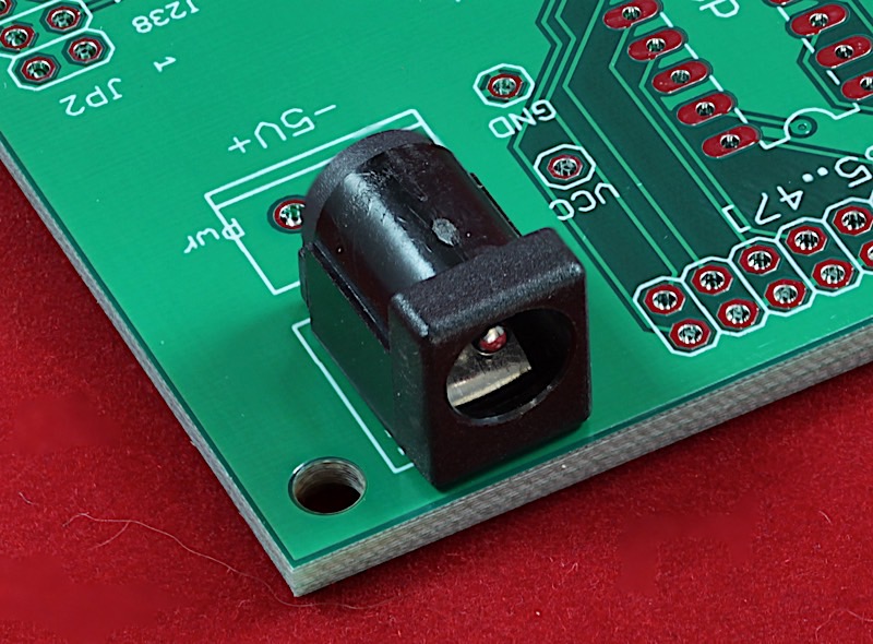
High resolution image
- The next step is to solder on all the dual row headers. There are eight 20-pin PPDIO headers (2x10) and three 14-pin SPI-6 bus headers (2x7).

High resolution image
- The last construction step is to install a jump on the RSTSEL (three-pin) header. Normally, you’ll install the jumper across the COM and RESET pins.
High resolution image
- At this point, soldering is largely complete (assuming you’ve made no mistakes that will require some rework). Turn the board over and slowly, careful, visually inspect every solder joint. Well over 50% of the failures I’ve had were due to missing a solder connection. It’s worthwhile to visually inspect all the pins (yeah, I know, there are a lot of them) to verify you haven’t missed any.
- If you installed sockets, a quick test to perform before installing the ICs is to apply power to the board and ensure the LED lights up. After that quick test, install the ICs.
WARNING: Please note that the MCP23S17 ICs are not all oriented the same way. Half of them are oriented up (that is, pin 1 is closest to the top of the board) while half of them are oriented down. This was down to make the board layout much cleaner. However, you have to watch yourself when installing the ICs to make sure the orientation matches that of the board.
See the note earlier about bending the pins on the ICs inward a bit.
- Now for the actual “smoke” test. With the ICs inserted, apply power and make sure the LED still lights up (no flickering!) and nothing gets overly hot (or worse, smokes and catches on fire! Yes, this has happened to me in the past).
- Assuming your board passes the “smoke” test, now it’s time to do a real test on the board. This will require running software on some device connected to the PPDIO96 board. The Plantation Productions, Inc., DAQ system has three boards that will suit this purpose: the DAQ_IF board (with a Netburner, Raspberry Pi, or Teensy 3.2 CPU module attached), the Weensy 3.6 board (with a Teensy 3.6 installed), or the Teensy-DAQ board (which is basically a Teensy 3.2 breakout board that includes an SPI-6 connector. For the purposes of this document, I’m using the DAQ-IF board with a Teensy 3.2 installed, because it’s easy to use. I have written a piece of PPDIO96 test software that runs on the Teensy/DAQ_IF (PPDIOTest.ino); this software was described a little earlier on this page.
- Before testing, make sure all the DIP switches (if you’ve installed them), are in the “off” position.
- The PPDIOTest.ino program continuously reads the 96 I/O inputs (as inputs) on the PPDIO96 board and displays their values as 8 sets of 3 hexadecimal digits (3 digits for every 12 bits). The software programs all the bits with polarity=0 and pullups enabled. Therefore, the program should display all “fff” characters if there are no pins shorted to ground. Now for the boring part--put a jumper on a ground pin (pin 2, 4, 5, 6, 10) and then on pin 2->1->3->5->7->9->11->13->15->7->19->20 (in succession). The corresponding hex values will be ffe, ffd, ffb, ff7, fef, fdf, fbf, f7f, eff, dff, bff, and 7ff, respectively, when you ground the corresponding pin.